
Datasheet


NXP Semiconductors
UM10973
LPCXpresso54114
UM10973
All information provided in this document is subject to legal disclaimers.
© NXP B.V. 2016. All rights reserved.
User manual
Rev. 1.1 — 25 February 2016
6 of 21
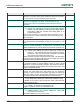
Circuit ref
Description
Ref section
J5
Target MCU Power / USB Device connector. Connect this micro USB B-type
connector to a +5V power source when it is desired to power only the Target
MCU, and leave the on-board Link2 debug probe unpowered.
n/a
J6
Link2 micro USB B-type connector. Powers both the Link2 side of the board
and LPC54114 Target side of the board. Power the board from this
connector when using the on-board debug probe to debug the LPC54114
Target MCU.
Table 2
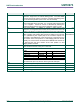
JP1
LPC54114 Target SWD disable – 2-position jumper pins.
1) Jumper open (default) the LPC54114 Target SWD interface
enabled. Normal operating mode where the Target SWD is
connected to either the on-board Link2 debug probe or an
external debug probe.
Jumper shunted, the LPC54114 Target SWD interface is disabled. Use this
setting only when the on-board Link2 debug probe is used to debug an off-
board Target MCU.
6
JP3
JP3 can be installed to reduce the voltage sense resistance (used by
the on-board current measurement circuitry) from 8.24 ohms to 4.12
ohms.
5.1
JP4
A current meter may be installed across JP4 terminals to measure the
LPC54114 current consumption. By default JP4 is shunted by a 0Ω
resistor installed at JS11; remove this shunt to measure current at JP4.
5.1.2
JP5
Link2 (LPC43xx) force DFU boot – 2 position jumper pins.
1) Jumper open (default) for Link2 to follow the normal boot
sequence. The Link2 will boot from internal flash if image is
found there. With the internal flash erased the Link2 normal
boot sequence will fall through to DFU boot.
Jumper shunted to force the Link2 to DFU boot mode. Use this setting
to reprogram the Link2 internal flash with a new image or to use the
LPCXpresso IDE with CMSIS-DAP protocol.
6.1.3
JP6
JP6 is used to isolate the Link2 debug probe (SPI bridge function) from
the LPC54114 target to prevent leakage current in power critical
applications / current consumption analysis. JP6 needs to be fitted to
use the SPI bridging function between the LPC54114 and Link2. This
jumper is not fitted by default.
n/a
JP7
On-board reset enable/disable. This jumper (not factory installed)
connects the reset button and reset signal from the expansion
connector J1 to the LPC54114 reset input. This jumper is shunted by
a zero ohm resistor on SJ9. This jumper is intended to be used when
an external host processor (controlling reset) is connected at J3.
n/a
JP8
Tri-color LED anode voltage enable:
1) By default JP8 is shunted by a 0Ω resistor installed at JS19.
To disable +3.3V to the tri-color led common anode, remove the 0Ω
resistor installed at JS19.
5.1 and 0
JP9
Power supply voltage selection – 3 position jumper pins.
1) Jumper 1–2: LPC54114 is powered at 1.8V.
Jumper 2–3 (default): LPC54114 is powered at 3.3V.
n/a
JP10
Target connector USB (J5) VBUS to LPC54114 connection:
1) Installed (default): JP10 connects VBUS from Target USB
connector to the LPC54114.
Not installed: VBUS from J5 is unconnected.
n/a