
Datasheet


NXP Semiconductors
UM10973
LPCXpresso54114
UM10973
All information provided in this document is subject to legal disclaimers.
© NXP B.V. 2016. All rights reserved.
User manual
Rev. 1.1 — 25 February 2016
5 of 21
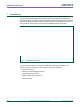
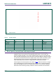
Fig 2. LPCXpresso54114 layout
The function of each identified component is listed in Table 1.
Table 1. Table Board interface components
Circuit ref
Description
Ref section
D1
Link2 LPC43xx BOOT0_LED indicator. Reflects the state of LPC43xx Link2
MCU P1_1. When the boot process fails, D1 will toggle at a 1 Hz rate for 60
seconds. After 60 seconds, the LPC43xx is reset.
0
D2
Tri-color LED driven by Target LPC54114 MCU. JP8 must be shunted for
+3.3V to be applied to D2 anode. The default shunt for JP8 is a 0Ω resistor
installed at JS19.
0
D3
Target LPC54114 Power LED.
0
D4
Target LPC54114 Reset LED – LED is on anytime the Target RESETn is
pulled low.
0
J1, J2, J8, J9
Expansion connectors, including Arduino Uno rev3 compatible connectivity.
8
J3
External processor control header. This connector provides access to the
LPC54114 control and ISP0 boot control to enable an external device control
reset and entry into I2C/SPI boot mode.
n/a
J4
PMod™ (SPI / I
2
C) Bridge connector. An external Application Processor (AP)
or PMod™ peripheral may be connected to the LPC54114 Target MCU SPI
and I2C via this connector.
8
D1
D2
D3
D4