
Datasheet


NXP Semiconductors
UM10973
LPCXpresso54114
UM10973
All information provided in this document is subject to legal disclaimers.
© NXP B.V. 2016. All rights reserved.
User manual
Rev. 1.1 — 25 February 2016
4 of 21
2. Feature summary
The LPCXpresso54114 board includes the following features:
On-board, high-speed USB based, Link2 debug probe with ARM’s CMSIS-DAP and
SEGGER J-Link protocol options.
Link2 probe can be used with on-board LPC54114 or external target.
Support for external debug probes.
Tri-color LED.
Target Reset, ISP, and WAKE buttons.
Expansion options based on Arduino UNO and PMod™, plus additional expansion
port pins.
On-board 1.8/3.3V or external power supply options.
Built-in power consumption measurement.
UART, I
2
C and SPI port bridging from LPC54114 target to USB via the on-board
debug probe.
8Mb Macronix MX25R SPI flash.
FTDI UART connector.
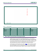
2.1 Board layout and settings
This section provides a quick reference guide to the main board components,
configurable items, visual indicators and expansion connectors. The layout of the
components on the LPCXpresso54114 board is shown in Fig 2.