
Datasheet


NXP Semiconductors
UM10973
LPCXpresso54114
UM10973
All information provided in this document is subject to legal disclaimers.
© NXP B.V. 2016. All rights reserved.
User manual
Rev. 1.1 — 25 February 2016
16 of 21
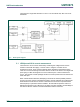
Table 4. Expansion connectors
Reference
Description
J1
The odd number pins are compatible with Arduino Uno rev3 Digital
15:8, AREF, SDA & SCL connector. The even numbered pins are
used for external access and expansion of LPC54114 signals not
used by the Arduino Uno rev3 compatible interface.
J2
The odd numbered pins 1 – 13 are compatible with Arduino Uno rev3
Digital 7:0 connector. The even numbered pins, and odd numbered
pins 17 and 19, are used for external access and expansion of
LPC54114 signals not used by the Arduino Uno rev3 compatible
interface.
J3
PMod™ connector. Connected to the LPC54114 Target MCU SPI0
and I2C2.
J8
The even numbered pins 6 – 20 are compatible with Arduino Uno
rev3 Power connector. The odd numbered pins, and even numbered
pins 2 and 4 are used.
J9
The even numbered pins 2 – 12 are compatible with Arduino Uno
rev3 Analog connector. The odd numbered pins are used for
external access and expansion of LPC54114 signals not used by the
Arduino Uno rev3 compatible interface.
9. Buttons
The LPCXpresso54114 board has 4 push buttons available to control the operation of the
LPC54114 (target) MCU. Their functions are as described below.
9.1 Reset
This button is used to reset the LPC54114 (note that the Link2 is NOT reset by this
button.)
9.2 ISP0 and ISP1
These button connect to the LPC54114 P0_31 (ISP0 button) and P0_4 (ISP1 button) pin
and may be used to force the LPC54114 into its various ISP boot modes. See Table 5.
Table 5. ISP boot mode control
Boot mode
ISP0
ISP1
Vbus (from J5)
I2C/SPI boot
Pressed
Pressed
X
UART boot
Pressed
Not pressed
0
USB Mass storage
Pressed
Not pressed
1
Boot from internal flash
Not pressed
Not pressed