
Datasheet


NXP Semiconductors
UM10973
LPCXpresso54114
UM10973
All information provided in this document is subject to legal disclaimers.
© NXP B.V. 2016. All rights reserved.
User manual
Rev. 1.1 — 25 February 2016
13 of 21
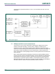
Fig 5. Current measurement circuit error
5.1.4 Shield board current measurement
To use the on-board current measurement circuitry, any expansion board must match the
functionality of the LPCXpresso54114. Refer to the board schematics for more
information.
6. Debug Configurations
The LPCXpresso54114 LQFP board has a built-in debug probe referred to as “Link2”.
The LPC54114 target MCU can be debugged by the Link2 debugging probe, or from an
external debug probe installed at P1. On-board jumpers JP1 and JP2 must be correctly
positioned for each mode. The on-board Link2 debug probe is capable of debugging
target MCU’s with a VDDIO range of 1.6V to 3.6V. Use JP9 to set the LPC54114 chip
VDD to the desired voltage level (+1.8V or +3.3V). Check the sections below for the
appropriate jumper settings and how to properly power the board.
% Error
LPC54114 current (µA)