
Datasheet


NXP Semiconductors
UM10973
LPCXpresso54114
UM10973
All information provided in this document is subject to legal disclaimers.
© NXP B.V. 2016. All rights reserved.
User manual
Rev. 1.1 — 25 February 2016
10 of 21
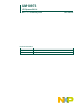
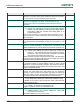
Fig 3. FTDI connector
Table 2. P3 FTDI interface
LPC54114 Signal
FTDI signal
Pin #
Direction
LPC54114 Signal
GND
GND
1
GND
No connect
CTS
2
No connect
Board +5V
5V
3
Board +5V
UART0_RXD
TXD
4
From host
UART0_RXD
UART0_TXD
RXD
5
To host
UART0_TXD
No connect
RTS
6
GND
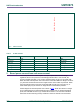
5. Board power connections and measurement
The LPCXpresso54114 board requires +5V input to power the on-board voltage
regulators which in turn power the Link2 debug probe and other +3.3V circuits, the
LPC54114 target and other +1.8V circuits, and the Arduino +5V and +3.3V power rails.
When the main external power source is from the Link2 side USB micro B-type connector
(J7), both the Link side and LPC54114 Target sections of the board are powered. When
the main external power is from the Target side USB micro B-type connector (J5), or
FTDI header (P3) only the LPC54114 Target section of the board is powered.
A block diagram of the board power tree is shown in Fig 4. When the LPC54114 Target
is to be debugged from an external debug probe, instead of the on-board Link2 debug
probe, the Link USB connector (J7) must be disconnected. The circle with I indicates
where the current monitoring circuitry measures / where an ammeter can be inserted.
1
2
3
4
5
6