
Datasheet
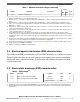
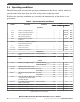

Table 1. Absolute maximum ratings (continued)
Symbol Parameter Conditions
1
Value
Unit
Min Max
MSL Moisture sensitivity level
11
— — 3 —
1. Voltages are referred to V
SS
if not specified otherwise
2. Allowed 1.45 V – 1.5 V for 60 seconds cumulative time at maximum T
J
= 150 °C; remaining time as defined in note 3 and
note 4
3. Allowed 1.375 V – 1.45 V for 10 hours cumulative time at maximum T
J
= 150 °C; remaining time as defined in note 4
4. 1.32 V – 1.375 V range allowed periodically for supply with sinusoidal shape and average supply value below 1.275 V at
maximum T
J
= 150 °C
5. Allowed 5.5 V – 6.0 V for 60 seconds cumulative time with no restrictions, for 10 hours cumulative time device in reset, T
J
= 150 °C; remaining time at or below 5.5 V
6. Allowed 3.6 V – 4.5 V for 60 seconds cumulative time with no restrictions, for 10 hours cumulative time device in reset, T
J
= 150 °C; remaining time at or below 3.6 V
7. The maximum input voltage on an I/O pin tracks with the associated I/P supply maximum. For the injection current
condition on a pin, the voltage will be equal to the supply plus the voltage drop across the internal ESD diode from I/O pin
to supply. The diode voltage varies greatly across process and temperature, but a value of 0.3V can be used for nominal
calculations.
8. The sum of all controller pins (including both digital and analog) must not exceed 200 mA. A V
DDEx
/V
DDEHx
power segment
is defined as one or more GPIO pins located between two V
DDEx
/V
DDEHx
supply pins.
9. The average current values given in I/O pad current specifications should be used to calculate total I/O segment current.
10. Solder profile per IPC/JEDEC J-STD-020D
11. Moisture sensitivity per JEDEC test method A112
3.2 Electromagnetic interference (EMI) characteristics
Test reports with EMC measurements to IC-level IEC standards are available on request.
To find application notes that provide guidance on designing your system to minimize
interference from radiated emissions, go to nxp.com and perform a keyword search for
"radiated emissions."
3.3 Electrostatic discharge (ESD) characteristics
Table 2. ESD Ratings
1, 2
Symbol Parameter Conditions Value Unit
V
HBM
ESD for Human Body Model (HBM) All pins 2000 V
V
CDM
ESD for Charged Device Model (CDM) Corner pins 750 V
Non-corner pins 500
1. All ESD testing is in conformity with CDF-AEC-Q100 Stress Test Qualification for Automotive Grade Integrated Circuits.
2. A device will be defined as a failure if after exposure to ESD pulses the device no longer meets the device specification
requirements.
Electrical characteristics
MPC5777C Microcontroller Data Sheet Data Sheet, Rev. 13, 08/2018.
NXP Semiconductors 9