
Datasheet
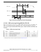
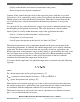
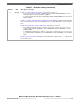

REF_CLK (input)
TXD[1:0] (outputs)
TX_EN
R7
R5
R6
R8
Figure 46. RMII transmit signal timing diagram
4 Package information
To find the package drawing for each package, go to http://www.nxp.com and perform a
keyword search for the drawing’s document number:
If you want the drawing for this package Then use this document number
416-ball MAPBGA 98ASA00562D
516-ball MAPBGA 98ASA00623D
4.1 Thermal characteristics
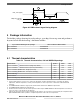
Table 54. Thermal characteristics, 416-ball MAPBGA package
Characteristic Symbol Value Unit
Junction to Ambient
1, 2
Natural Convection (Single layer board) R
ΘJA
28.8 °C/W
Junction to Ambient
1, 3
Natural Convection (Four layer board 2s2p) R
ΘJA
19.6 °C/W
Junction to Ambient (@200 ft./min., Single layer board) R
ΘJMA
21.3 °C/W
Junction to Ambient (@200 ft./min., Four layer board 2s2p) R
ΘJMA
15.1 °C/W
Junction to Board
4
R
ΘJB
9.5 °C/W
Junction to Case
5
R
ΘJC
4.8 °C/W
Junction to Package Top
6
Natural Convection Ψ
JT
0.2 °C/W
1. Junction temperature is a function of on-chip power dissipation, package thermal resistance, mounting site (board)
temperature, ambient temperature, air flow, power dissipation of other components on the board, and board thermal
resistance.
2. Per JEDEC JESD51-2 with the single layer board horizontal. Board meets JESD51-9 specification.
3. Per JEDEC JESD51-6 with the board horizontal.
4. Thermal resistance between the die and the printed circuit board per JEDEC JESD51-8. Board temperature is measured
on the top surface of the board near the package.
5. Indicates the average thermal resistance between the die and the case top surface as measured by the cold plate method
(MIL SPEC-883 Method 1012.1) with the cold plate temperature used for the case temperature.
Package information
MPC5777C Microcontroller Data Sheet Data Sheet, Rev. 13, 08/2018.
NXP Semiconductors 83