
Datasheet
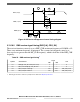
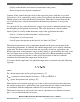
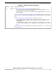

REF_CLK (input)
RXD[1:0] (inputs)
CRS_DV
R1
R2
R4
R3
Figure 45. RMII receive signal timing diagram
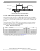
3.13.10.6 RMII transmit signal timing (TXD[1:0], TX_EN)
The transmitter functions correctly up to a REF_CLK maximum frequency of 50 MHz +
1%. There is no minimum frequency requirement. The system clock frequency must be at
least equal to or greater than the TX_CLK frequency, which is half that of the REF_CLK
frequency.
The transmit outputs (TXD[1:0], TX_EN) can be programmed to transition from either
the rising or falling edge of REF_CLK, and the timing is the same in either case. This
options allows the use of non-compliant RMII PHYs.
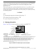
Table 53. RMII transmit signal timing
1
Symbol Characteristic
Value
2
Unit
Min Max
R5 REF_CLK to TXD[1:0], TX_EN invalid 2 — ns
R6 REF_CLK to TXD[1:0], TX_EN valid — 16 ns
R7 REF_CLK pulse width high 35% 65% REF_CLK period
R8 REF_CLK pulse width low 35% 65% REF_CLK period
1. All timing specifications valid to the pad input levels defined in I/O pad specifications.
2. Output parameters are valid for C
L
= 25 pF, where C
L
is the external load to the device. The internal package capacitance
is accounted for, and does not need to be subtracted from the 25 pF value.
Electrical characteristics
MPC5777C Microcontroller Data Sheet Data Sheet, Rev. 13, 08/2018.
82 NXP Semiconductors