
Datasheet
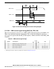
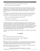
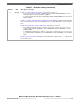

MDC (output)
M12
M13
M11
M14
MDIO (output)
MDIO (input)
M15
M10
Figure 44. MII serial management channel timing diagram
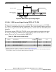
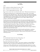
3.13.10.5 RMII receive signal timing (RXD[1:0], CRS_DV)
The receiver functions correctly up to a REF_CLK maximum frequency of 50 MHz +1%.
There is no minimum frequency requirement. The system clock frequency must be at
least equal to or greater than the RX_CLK frequency, which is half that of the REF_CLK
frequency.
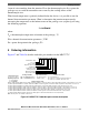
Table 52. RMII receive signal timing
1
Symbol Characteristic
Value
Unit
Min Max
R1 RXD[1:0], CRS_DV to REF_CLK setup 4 — ns
R2 REF_CLK to RXD[1:0], CRS_DV hold 2 — ns
R3 REF_CLK pulse width high 35% 65% REF_CLK period
R4 REF_CLK pulse width low 35% 65% REF_CLK period
1. All timing specifications valid to the pad input levels defined in I/O pad specifications.
Electrical characteristics
MPC5777C Microcontroller Data Sheet Data Sheet, Rev. 13, 08/2018.
NXP Semiconductors 81