
Datasheet
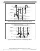
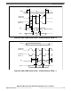
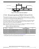

TX_CLK (input)
TXD[3:0] (outputs)
TX_EN
M7
M5
M6
M8
Figure 42. MII transmit signal timing diagram
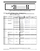
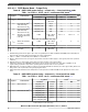
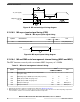
3.13.10.3 MII async inputs signal timing (CRS)
Table 50. MII async inputs signal timing
Symbol Characteristic
Value
Unit
Min Max
M9 CRS minimum pulse width 1.5 — TX_CLK period
CRS
M9
Figure 43. MII async inputs timing diagram
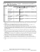
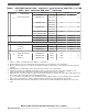
3.13.10.4 MII and RMII serial management channel timing (MDIO and MDC)
The FEC functions correctly with a maximum MDC frequency of 2.5 MHz.
Table 51. MII serial management channel timing
1
Symbol Characteristic
Value
2
Unit
Min Max
M10 MDC falling edge to MDIO output invalid (minimum
propagation delay)
0 — ns
M11 MDC falling edge to MDIO output valid (max prop delay) — 25 ns
M12 MDIO (input) to MDC rising edge setup 10 — ns
M13 MDIO (input) to MDC rising edge hold 0 — ns
M14 MDC pulse width high 40% 60% MDC period
M15 MDC pulse width low 40% 60% MDC period
1. All timing specifications valid to the pad input levels defined in I/O pad specifications.
2. Output parameters are valid for C
L
= 25 pF, where C
L
is the external load to the device. The internal package capacitance
is accounted for, and does not need to be subtracted from the 25 pF value
Electrical characteristics
MPC5777C Microcontroller Data Sheet Data Sheet, Rev. 13, 08/2018.
80 NXP Semiconductors