
Datasheet
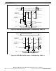
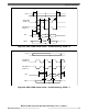

PCSx
t
SUO
SCK Output
(CPOL = 0)
SOUT
First Data
Data
Last Data
t
HO
t
SCK
t
CSH
t
SDC
t
CSV
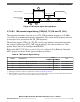
Figure 40. DSPI LVDS and CMOS master timing – output only – modified transfer format
MTFE = 1, CHPA = 1
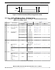
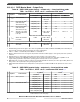
3.13.10 FEC timing
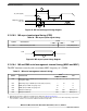
3.13.10.1 MII receive signal timing (RXD[3:0], RX_DV, and RX_CLK)
The receiver functions correctly up to a RX_CLK maximum frequency of 25 MHz +1%.
There is no minimum frequency requirement. The system clock frequency must be at
least equal to or greater than the RX_CLK frequency.
Table 48. MII receive signal timing
1
Symbol Characteristic
Value
Unit
Min Max
M1 RXD[3:0], RX_DV to RX_CLK setup 5 — ns
M2 RX_CLK to RXD[3:0], RX_DV hold 5 — ns
M3 RX_CLK pulse width high 35% 65% RX_CLK period
M4 RX_CLK pulse width low 35% 65% RX_CLK period
1. All timing specifications valid to the pad input levels defined in I/O pad current specifications.
Electrical characteristics
MPC5777C Microcontroller Data Sheet Data Sheet, Rev. 13, 08/2018.
78 NXP Semiconductors