
Datasheet
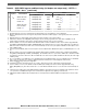
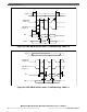
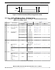
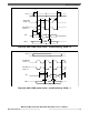
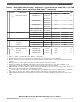
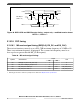
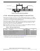

Table 45. DSPI LVDS master timing – full duplex – modified transfer format (MTFE = 1),
CPHA = 0 or 1 (continued)
# Symbol Characteristic
Condition
1
Value
2
Unit
Pad drive
3
Load (C
L
) Min Max
9 t
SUO
SOUT data valid time (after SCK edge)
SOUT data valid
time from SCK
CPHA = 0
10
LVDS 15 pF to 25 pF
differential
— 7.0 + t
SYS
5
ns
SOUT data valid
time from SCK
CPHA = 1
10
LVDS 15 pF to 25 pF
differential
— 7.0 ns
10 t
HO
SOUT data hold time (after SCK edge)
SOUT data hold
time after SCK
CPHA = 0
10
LVDS 15 pF to 25 pF
differential
–7.5 + t
SYS
5
— ns
SOUT data hold
time after SCK
CPHA = 1
10
LVDS 15 pF to 25 pF
differential
–7.5 — ns
1. When a characteristic involves two signals, the pad drive and load conditions apply to each signal's pad, unless specified
otherwise.
2. All timing values for output signals in this table are measured to 50% of the output voltage.
3. Pad drive is defined as the PCR[SRC] field setting in the SIU. Timing is guaranteed to same drive capabilities for all
signals; mixing of pad drives may reduce operating speeds and may cause incorrect operation.
4. N is the number of clock cycles added to time between PCS assertion and SCK assertion and is software programmable
using DSPI_CTARx[PSSCK] and DSPI_CTARx[CSSCK]. The minimum value is 2 cycles unless TSB mode or Continuous
SCK clock mode is selected, in which case, N is automatically set to 0 clock cycles (PCS and SCK are driven by the same
edge of DSPI_CLKn).
5. t
SYS
is the period of DSPI_CLKn clock, the input clock to the DSPI module. Maximum frequency is 100 MHz (min tSYS =
10 ns).
6. M is the number of clock cycles added to time between SCK negation and PCS negation and is software programmable
using DSPI_CTARx[PASC] and DSPI_CTARx[ASC]. The minimum value is 2 cycles unless TSB mode or Continuous SCK
clock mode is selected, in which case, M is automatically set to 0 clock cycles (PCS and SCK are driven by the same edge
of DSPI_CLKn).
7. t
SDC
is only valid for even divide ratios. For odd divide ratios the fundamental duty cycle is not 50:50. For these odd divide
ratios cases, the absolute spec number is applied as jitter/uncertainty to the nominal high time and low time.
8. Input timing assumes an input slew rate of 1 ns (10% – 90%) and LVDS differential voltage = ±100 mV.
9. P is the number of clock cycles added to delay the DSPI input sample point and is software programmable using
DSPI_MCR[SMPL_PT]. The value must be 0, 1 or 2. If the baud rate divide ratio is /2 or /3, this value is automatically set
to 1.
10. SOUT Data Valid and Data hold are independent of load capacitance if SCK and SOUT load capacitances are the same
value.
Electrical characteristics
MPC5777C Microcontroller Data Sheet Data Sheet, Rev. 13, 08/2018.
74 NXP Semiconductors