
Datasheet
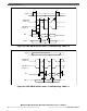
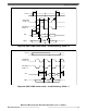
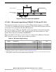

PCSS
PCSx
tPCSC
tPASC
Figure 37. DSPI PCS strobe (PCSS) timing (master mode)
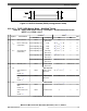
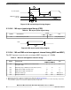
3.13.9.1.3 DSPI LVDS Master Mode – Modified Timing
Table 45. DSPI LVDS master timing – full duplex – modified transfer format
(MTFE = 1), CPHA = 0 or 1
# Symbol Characteristic
Condition
1
Value
2
Unit
Pad drive
3
Load (C
L
) Min Max
1 t
SCK
SCK cycle time LVDS 15 pF to 25 pF
differential
33.3 — ns
2 t
CSC
PCS to SCK delay
(LVDS SCK)
PCS: PCR[SRC]=11b 25 pF (N
4
× t
SYS
, 5
) – 10 — ns
PCS: PCR[SRC]=10b 50 pF (N
4
× t
SYS
, 5
) – 10 — ns
PCS: PCR[SRC]=01b 50 pF (N
4
× t
SYS
, 5
) – 32 — ns
3 t
ASC
After SCK delay
(LVDS SCK)
PCS: PCR[SRC]=11b PCS: 0 pF
SCK: 25 pF
(M
6
× t
SYS
, 5
) – 8 — ns
PCS: PCR[SRC]=10b PCS: 0 pF
SCK: 25 pF
(M
6
× t
SYS
, 5
) – 8 — ns
PCS: PCR[SRC]=01b PCS: 0 pF
SCK: 25 pF
(M
6
× t
SYS
, 5
) – 8 — ns
4 t
SDC
SCK duty cycle
7
LVDS 15 pF to 25 pF
differential
1/2t
SCK
– 2 1/2t
SCK
+2 ns
7 t
SUI
SIN setup time
SIN setup time to
SCK
CPHA = 0
8
LVDS 15 pF to 25 pF
differential
23 – (P
9
× t
SYS
, 5
) — ns
SIN setup time to
SCK
CPHA = 1
8
LVDS 15 pF to 25 pF
differential
23 — ns
8 t
HI
SIN hold time
SIN hold time from
SCK
CPHA = 0
8
LVDS 0 pF differential –1 + (P
9
× t
SYS
, 5
) — ns
SIN hold time from
SCK
CPHA = 1
8
LVDS 0 pF differential –1 — ns
Table continues on the next page...
Electrical characteristics
MPC5777C Microcontroller Data Sheet Data Sheet, Rev. 13, 08/2018.
NXP Semiconductors 73