
Datasheet


SCK clock mode is selected, in which case, N is automatically set to 0 clock cycles (PCS and SCK are driven by the same
edge of DSPI_CLKn).
6. t
SYS
is the period of DSPI_CLKn clock, the input clock to the DSPI module. Maximum frequency is 100 MHz (min t
SYS
= 10
ns).
7. M is the number of clock cycles added to time between SCK negation and PCS negation and is software programmable
using DSPI_CTARx[PASC] and DSPI_CTARx[ASC]. The minimum value is 2 cycles unless TSB mode or Continuous SCK
clock mode is selected, in which case, M is automatically set to 0 clock cycles (PCS and SCK are driven by the same edge
of DSPI_CLKn).
8. t
SDC
is only valid for even divide ratios. For odd divide ratios the fundamental duty cycle is not 50:50. For these odd divide
ratios cases, the absolute spec number is applied as jitter/uncertainty to the nominal high time and low time.
9. PCSx and PCSS using same pad configuration.
10. Input timing assumes an input slew rate of 1 ns (10% – 90%) and uses TTL / Automotive voltage thresholds.
11. SOUT Data Valid and Data hold are independent of load capacitance if SCK and SOUT load capacitances are the same
value.
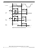
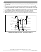
PCSx
t
SDC
SCK Output
(CPOL = 0)
SCK Output
(CPOL = 1)
SIN
SOUT
First Data
First Data
Data
Data
Last Data
Last Data
t
CSC
t
ASC
t
SCK
t
SDC
t
SUI
t
HI
t
SUO
t
HO
Figure 32. DSPI CMOS master mode – classic timing, CPHA = 0
Electrical characteristics
MPC5777C Microcontroller Data Sheet Data Sheet, Rev. 13, 08/2018.
68 NXP Semiconductors