
Datasheet
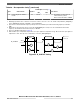

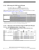

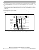


Table 43. DSPI CMOS master classic timing (full duplex and output only) – MTFE = 0, CPHA
= 0 or 1
1
(continued)
# Symbol Characteristic
Condition
2
Value
3
Unit
Pad drive
4
Load (C
L
) Min Max
3 t
ASC
After SCK delay PCR[SRC]=11b PCS: 0 pF
SCK: 50 pF
(M
7
× t
SYS
, 6
) – 35 — ns
PCR[SRC]=10b PCS: 0 pF
SCK: 50 pF
(M
7
× t
SYS
, 6
) – 35 —
PCR[SRC]=01b PCS: 0 pF
SCK: 50 pF
(M
7
× t
SYS
, 6
) – 35 —
PCS: PCR[SRC]=01b
SCK: PCR[SRC]=10b
PCS: 0 pF
SCK: 50 pF
(M
7
× t
SYS
, 6
) – 35 —
4 t
SDC
SCK duty cycle
8
PCR[SRC]=11b 0 pF 1/2t
SCK
– 2 1/2t
SCK
+ 2 ns
PCR[SRC]=10b 0 pF 1/2t
SCK
– 2 1/2t
SCK
+ 2
PCR[SRC]=01b 0 pF 1/2t
SCK
– 5 1/2t
SCK
+ 5
PCS strobe timing
5 t
PCSC
PCSx to PCSS
time
9
PCR[SRC]=10b 25 pF 13.0 — ns
6 t
PASC
PCSS to PCSx
time
9
PCR[SRC]=10b 25 pF 13.0 — ns
SIN setup time
7 t
SUI
SIN setup time to
SCK
10
PCR[SRC]=11b 25 pF 29.0 — ns
PCR[SRC]=10b 50 pF 31.0 —
PCR[SRC]=01b 50 pF 62.0 —
SIN hold time
8 t
HI
SIN hold time from
SCK
10
PCR[SRC]=11b 0 pF –1.0 — ns
PCR[SRC]=10b 0 pF –1.0 —
PCR[SRC]=01b 0 pF –1.0 —
SOUT data valid time (after SCK edge)
9 t
SUO
SOUT data valid
time from SCK
11
PCR[SRC]=11b 25 pF — 7.0 ns
PCR[SRC]=10b 50 pF — 8.0
PCR[SRC]=01b 50 pF — 18.0
SOUT data hold time (after SCK edge)
10 t
HO
SOUT data hold
time after SCK
11
PCR[SRC]=11b 25 pF –9.0 — ns
PCR[SRC]=10b 50 pF –10.0 —
PCR[SRC]=01b 50 pF –21.0 —
1. All output timing is worst case and includes the mismatching of rise and fall times of the output pads.
2. When a characteristic involves two signals, the pad drive and load conditions apply to each signal's pad, unless specified
otherwise.
3. All timing values for output signals in this table are measured to 50% of the output voltage.
4. Pad drive is defined as the PCR[SRC] field setting in the SIU. Timing is guaranteed to same drive capabilities for all
signals; mixing of pad drives may reduce operating speeds and may cause incorrect operation.
5. N is the number of clock cycles added to time between PCS assertion and SCK assertion and is software programmable
using DSPI_CTARx[PSSCK] and DSPI_CTARx[CSSCK]. The minimum value is 2 cycles unless TSB mode or Continuous
Electrical characteristics
MPC5777C Microcontroller Data Sheet Data Sheet, Rev. 13, 08/2018.
NXP Semiconductors 67