
Datasheet


3.13.9 DSPI timing with CMOS and LVDS pads
NOTE
The DSPI in TSB mode with LVDS pads can be used to
implement the Micro Second Channel (MSC) bus protocol.
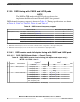
DSPI channel frequency support is shown in Table 42. Timing specifications are shown
in Table 43, Table 44, Table 45, Table 46, and Table 47.
Table 42. DSPI channel frequency support
DSPI use mode Max usable frequency (MHz)
1, 2
CMOS (Master mode) Full duplex – Classic timing (Table 43) 17
Full duplex – Modified timing (Table 44) 30
Output only mode (SCK/SOUT/PCS) (Table 43 and Table 44) 30
Output only mode TSB mode (SCK/SOUT/PCS) (Table 47) 30
LVDS (Master mode) Full duplex – Modified timing (Table 45) 30
Output only mode TSB mode (SCK/SOUT/PCS) (Table 46) 40
1. Maximum usable frequency can be achieved if used with fastest configuration of the highest drive pads.
2. Maximum usable frequency does not take into account external device propagation delay.
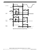
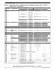
3.13.9.1 DSPI master mode full duplex timing with CMOS and LVDS pads
3.13.9.1.1 DSPI CMOS Master Mode — Classic Timing
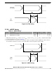
Table 43. DSPI CMOS master classic timing (full duplex and output only) –
MTFE = 0, CPHA = 0 or 1
1
# Symbol Characteristic
Condition
2
Value
3
Unit
Pad drive
4
Load (C
L
) Min Max
1 t
SCK
SCK cycle time PCR[SRC]=11b 25 pF 33.0 — ns
PCR[SRC]=10b 50 pF 80.0 —
PCR[SRC]=01b 50 pF 200.0 —
2 t
CSC
PCS to SCK delay PCR[SRC]=11b 25 pF (N
5
× t
SYS
, 6
) – 16 — ns
PCR[SRC]=10b 50 pF (N
5
× t
SYS
, 6
) – 16 —
PCR[SRC]=01b 50 pF (N
5
× t
SYS
, 6
) – 18 —
PCS: PCR[SRC]=01b
SCK: PCR[SRC]=10b
50 pF (N
5
× t
SYS
, 6
) – 45 —
Table continues on the next page...
Electrical characteristics
MPC5777C Microcontroller Data Sheet Data Sheet, Rev. 13, 08/2018.
66 NXP Semiconductors