
Datasheet


3.13.6 External interrupt timing (IRQ/NMI pin)
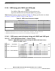
Table 39. External Interrupt timing
1
Spec Characteristic Symbol Min Max Unit
1 IRQ/NMI Pulse Width Low t
IPWL
3 — t
cyc
2
2 IRQ/NMI Pulse Width High t
IPWH
3 — t
cyc
2
3 IRQ/NMI Edge to Edge Time
3
t
ICYC
6 — t
cyc
2
1. IRQ/NMI timing specified at V
DD
= 1.08 V to 1.32 V, V
DDEH
= 3.0 V to 5.5 V, T
A
= T
L
to T
H
.
2. For further information on t
cyc
, see Table 3.
3. Applies when IRQ/NMI pins are configured for rising edge or falling edge events, but not both.
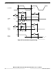
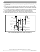
IRQ
3
1 2
Figure 29. External interrupt timing
3.13.7 eTPU timing
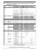
Table 40. eTPU timing
1
Spec Characteristic Symbol Min Max Unit
1 eTPU Input Channel Pulse Width t
ICPW
4 — t
CYC_ETPU
2
2 eTPU Output Channel Pulse Width t
OCPW
1
3
— t
CYC_ETPU
2
1. eTPU timing specified at V
DD
= 1.08 V to 1.32 V, V
DDEH
= 3.0 V to 5.5 V, T
A
= T
L
to T
H
, and C
L
= 200 pF with SRC = 0b00.
2. For further information on
tCYC_ETPU
, see Table 3.
3. This specification does not include the rise and fall times. When calculating the minimum eTPU pulse width, include the
rise and fall times defined in the slew rate control fields (SRC) of the pad configuration registers (PCR).
Electrical characteristics
MPC5777C Microcontroller Data Sheet Data Sheet, Rev. 13, 08/2018.
64 NXP Semiconductors