
Datasheet
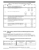
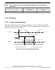
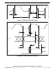
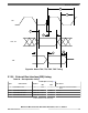
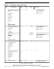

Table 37. Nexus debug port timing
1
(continued)
Spec Characteristic Symbol Min Max Unit
8 Absolute minimum TCK cycle time
4
(TDO sampled on
posedge of TCK)
t
TCYC
40
5
— ns
Absolute minimum TCK cycle time
4
(TDO sampled on
negedge of TCK)
20
5
—
9 TCK Duty Cycle t
TDC
40 60 %
10 TDI, TMS Data Setup Time
6
t
NTDIS
, t
NTMSS
8 — ns
11 TDI, TMS Data Hold Time
6
T
NTDIH
, t
NTMSH
5 — ns
12 TCK Low to TDO Data Valid
6
t
NTDOV
0 18 ns
13 RDY Valid to MCKO
7
— — — —
14 TDO hold time after TCLK low
6
t
NTDOH
1 — ns
1. All Nexus timing relative to MCKO is measured from 50% of MCKO and 50% of the respective signal. Nexus timing
specified at V
DD
= 1.08 V to 1.32 V, V
DDE
= 3.0 V to 3.6 V, V
DD33
and V
DDSYN
= 3.0 V to 3.6 V, T
A
= T
L
to T
H
, and C
L
= 30
pF with DSC = 0b10.
2. MDO, MSEO, and EVTO data is held valid until next MCKO low cycle.
3. This is a functionally allowable feature. However, it may be limited by the maximum frequency specified by the absolute
minimum TCK period specification.
4. This value is TDO propagation time plus 2 ns setup time to sampling edge.
5. This may require a maximum clock speed that is less than the maximum functional capability of the design depending on
the actual system frequency being used.
6. Applies to TMS pin timing for the bit frame when using the 1149.7 advanced protocol.
7. The RDY pin timing is asynchronous to MCKO. The timing is guaranteed by design to function correctly.
MCKO
Output Data Valid
MDO
MSEO
EVTO
EVTI
1
2
3
4
5
6
7
Figure 23. Nexus timings
Electrical characteristics
MPC5777C Microcontroller Data Sheet Data Sheet, Rev. 13, 08/2018.
58 NXP Semiconductors