
Datasheet
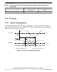
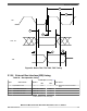

RESET
2
1
RSTOUT
PLLCFG
BOOTCFG
WKPCFG
4
3
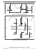
Figure 18. Reset and configuration pin timing
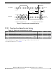
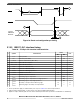
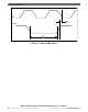
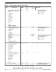
3.13.3 IEEE 1149.1 interface timing
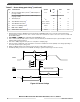
Table 36. JTAG pin AC electrical characteristics
1
# Symbol Characteristic
Value
Unit
Min Max
1 t
JCYC
TCK cycle time 100 — ns
2 t
JDC
TCK clock pulse width 40 60 %
3 t
TCKRISE
TCK rise and fall times (40%–70%) — 3 ns
4 t
TMSS
, t
TDIS
TMS, TDI data setup time 5 — ns
5 t
TMSH
, t
TDIH
TMS, TDI data hold time 5 — ns
6 t
TDOV
TCK low to TDO data valid — 16
2
ns
7 t
TDOI
TCK low to TDO data invalid 0 — ns
8 t
TDOHZ
TCK low to TDO high impedance — 15 ns
9 t
JCMPPW
JCOMP assertion time 100 — ns
10 t
JCMPS
JCOMP setup time to TCK low 40 — ns
11 t
BSDV
TCK falling edge to output valid — 600
3
ns
12 t
BSDVZ
TCK falling edge to output valid out of high impedance — 600 ns
13 t
BSDHZ
TCK falling edge to output high impedance — 600 ns
14 t
BSDST
Boundary scan input valid to TCK rising edge 15 — ns
15 t
BSDHT
TCK rising edge to boundary scan input invalid 15 — ns
1. These specifications apply to JTAG boundary scan only. See Table 37 for functional specifications.
2. Timing includes TCK pad delay, clock tree delay, logic delay and TDO output pad delay.
3. Applies to all pins, limited by pad slew rate. Refer to I/O delay and transition specification and add 20 ns for JTAG delay.
Electrical characteristics
MPC5777C Microcontroller Data Sheet Data Sheet, Rev. 13, 08/2018.
54 NXP Semiconductors