
Datasheet
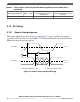
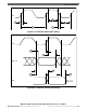
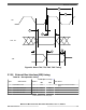

D_CLKOUT
I/O Inputs
B
A
A – Maximum Input Delay Time
B – Minimum Input Hold Time
V
DDE /
2
V
DDEn / 2
V
DDEHn / 2
Figure 17. Generic input setup/hold timing
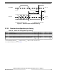
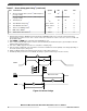
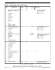
3.13.2 Reset and configuration pin timing
Table 35. Reset and configuration pin timing
1
Spec Characteristic Symbol Min Max Unit
1 RESET Pulse Width t
RPW
10 — t
cyc
2
2 RESET Glitch Detect Pulse Width t
GPW
2 — t
cyc
2
3 PLLCFG, BOOTCFG, WKPCFG Setup Time to RSTOUT Valid t
RCSU
10 — t
cyc
2
4 PLLCFG, BOOTCFG, WKPCFG Hold Time to RSTOUT Valid t
RCH
0 — t
cyc
2
1. Reset timing specified at: V
DDEH
= 3.0 V to 5.25 V, V
DD
= 1.08 V to 1.32 V, TA = TL to TH.
2. For further information on t
cyc
, see Table 3.
Electrical characteristics
MPC5777C Microcontroller Data Sheet Data Sheet, Rev. 13, 08/2018.
NXP Semiconductors 53