
Datasheet
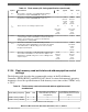
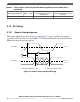
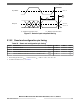
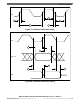
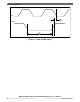
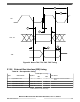
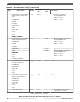

Table 34. Flash memory read wait-state and address-pipeline control combinations
(continued)
Flash memory frequency RWSC APC
Flash memory read latency on
mini-cache miss (# of f
PLATF
clock periods)
Flash memory read latency on
mini-cache hit (# of f
PLATF
clock
periods)
100 MHz < f
PLATF
≤ 150 MHz 3 1 6 1
3.13 AC timing
3.13.1 Generic timing diagrams
The generic timing diagrams in Figure 16 and Figure 17 apply to all I/O pins with pad
types SR and FC. See the associated MPC5777C Microsoft Excel® file in the Reference
Manual for the pad type for each pin.
D_CLKOUT
I/O Outputs
B
A
A – Maximum Output Delay Time
B – Minimum Output Hold Time
V
DDE /
2
V
DDEn / 2
V
DDEHn / 2
Figure 16. Generic output delay/hold timing
Electrical characteristics
MPC5777C Microcontroller Data Sheet Data Sheet, Rev. 13, 08/2018.
52 NXP Semiconductors