
Datasheet
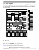
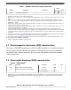

1.2 Block diagram
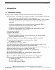
The following figure shows a top-level block diagram of the MPC5777C. The purpose of
the block diagram is to show the general interconnection of functional modules through
the crossbar switch.
COMPUTATIONAL SHELL
e200z7
(dual issue)
SWT
STM
INTC
FPU
VLE
16K I-Cache
16K D-Cache
MMU
e200z7 checker
core complex
DEBUG
JTAG
MMU
Nexus 3+
DTS
64ch eDMA
64ch eDMA
Ethernet
Crossbar Switch with ECC
MPU
Safety
Monitor
SRAM
SRAM
Control
Tamper
Detection
CSE
Bridge B
Bridge A
Flash Control
Flash w/ EEPROM
EBI
Security
FLEXCAN_A-B
MCAN_0-1
DSPI_A-C
eSCI_A-C
ETPU_C
w/RAM
eMIOS_0
eQADC_A
& Temp Sensors
DECFILTER_A-L
SDADC_1/3
SRX_0
PSI5_0
REACM2
Zipwire/
SIPI/LFAST
Dual PLL/
OSC/IRC
CRC
PCM/ERM
SIU/SIU_B
CMU_0-8
EBI registers
FCCU
STCU
PMU/PMC
PIT-RTI
FlexCAN_C-D
DSPI_D-E
eSCI_D-F
ETPU_A/B
(w/RAM)
eMIOS_1
eQADC_B
SDADC_2/4
SRX_1
PSI5_1
e200z7
(dual issue)
FPU
VLE
16K I-Cache
16K D-Cache
MMU
SWT
STM
INTC
Figure 1. MPC5777C block diagram
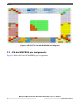
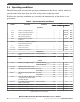
Pinouts
2.1 416-ball MAPBGA pin assignments
Figure 2 shows the 416-ball MAPBGA pin assignments.
2
Pinouts
MPC5777C Microcontroller Data Sheet Data Sheet, Rev. 13, 08/2018.
NXP Semiconductors 5