
Datasheet
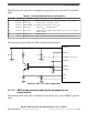
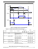
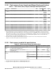

Table 29. Voltage monitor electrical characteristics
1, 2
(continued)
Symbol Parameter Conditions
Configuration Value
Unit
Trim
bits
Mask
Opt.
Pow.
Up
Min Typ Max
POR_HV HV V
DDPMC
supply power
on reset threshold
Rising voltage (powerup) N/A No Enab. 2444 2600 2756 mV
Falling voltage (power
down)
2424 2580 2736
LVD_HV HV internal V
DDPMC
supply
low voltage monitoring
Rising voltage (untrimmed) 4bit No Enab. 2935 3023 3112 mV
Falling voltage (untrimmed) 2922 3010 3099
Rising voltage (trimmed) 2946 3010 3066
Falling voltage (trimmed) 2934 2998 3044
HVD_HV HV internal V
DDPMC
supply
high voltage monitoring
Rising voltage 4bit Yes Disab. 5696 5860 5968 mV
Falling voltage 5666 5830 5938
LVD_FLASH FLASH supply low voltage
monitoring
6
Rising voltage (untrimmed) 4bit No Enab. 2935 3023 3112 mV
Falling voltage (untrimmed) 2922 3010 3099
Rising voltage (trimmed) 2956 3010 3053
Falling voltage (trimmed) 2944 2998 3041
HVD_FLASH FLASH supply high
voltage monitoring
6
Rising voltage 4bit Yes Disab. 3456 3530 3584 mV
Falling voltage 3426 3500 3554
LVD_IO Main I/O V
DDEH1
supply
low voltage monitoring
Rising voltage (untrimmed) 4bit No Enab. 3250 3350 3488 mV
Falling voltage (untrimmed) 3220 3320 3458
Rising voltage (trimmed) 3347 3420 3468
Falling voltage (trimmed) 3317 3390 3438
t
VDASSERT
Voltage detector threshold
crossing assertion
— — — — 0.1 — 2.0 μs
t
VDRELEASE
Voltage detector threshold
crossing de-assertion
— — — — 5 — 20 μs
1. LVD is released after t
VDRELEASE
temporization when upper threshold is crossed; LVD is asserted t
VDASSERT
after detection
when lower threshold is crossed.
2. HVD is released after t
VDRELEASE
temporization when lower threshold is crossed; HVD is asserted t
VDASSERT
after
detection when upper threshold is crossed.
3. POR098_c threshold is an untrimmed value, before the completion of the power-up sequence. All other LVD/HVD
thresholds are provided after trimming.
4. LV internal supply levels are measured on device internal supply grid after internal voltage drop.
5. LV external supply levels are measured on the die side of the package bond wire after package voltage drop.
6. V
DDFLA
range is guaranteed when internal flash memory regulator is used.
3.11.4 Power sequencing requirements
Requirements for power sequencing include the following.
Electrical characteristics
MPC5777C Microcontroller Data Sheet Data Sheet, Rev. 13, 08/2018.
46 NXP Semiconductors