
Datasheet
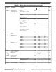
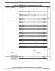
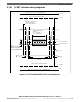
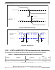
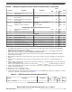
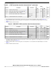
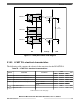

Table 21. LFAST transmitter electrical characteristics
1
(continued)
Symbol Parameter Conditions
Value
Unit
Min Typ Max
V
OS
Common mode voltage — 1.08 — 1.32 V
|V
OD
| Differential output voltage swing (terminated)
2
,
3
— 110 200 285 mV
t
TR
Rise/fall time (10% – 90% of swing)
2
,
3
— 0.26 — 1.5 ns
C
L
External lumped differential load capacitance
2
V
DDE
= 4.5 V — — 12.0 pF
V
DDE
= 3.0 V — — 8.5
I
LVDS_TX
Transmitter DC current consumption Enabled — — 3.2 mA
1. The LFAST pad electrical characteristics are based on worst-case internal capacitance values shown in Figure 11.
2. Valid for maximum data rate f
DATA
. Value given is the capacitance on each terminal of the differential pair, as shown in
Figure 11.
3. Valid for maximum external load CL.
Table 22. MSC/DSPI LVDS transmitter electrical characteristics
1
Symbol Parameter Conditions
Value
Unit
Min Typ Max
f
DATA
Data rate — — — 80 Mbps
V
OS
Common mode voltage — 1.08 — 1.32 V
|V
OD
| Differential output voltage swing (terminated)
2
,
3
— 150 200 400 mV
t
TR
Rise/Fall time (10%–90% of swing)
2
,
3
— 0.8 — 4.0 ns
C
L
External lumped differential load capacitance
2
V
DDE
= 4.5 V — — 50 pF
V
DDE
= 3.0 V — — 39
I
LVDS_TX
Transmitter DC current consumption Enabled — — 4.0 mA
1. The MSC and DSPI LVDS pad electrical characteristics are based on the application circuit and typical worst-case internal
capacitance values given in Figure 11.
2. Valid for maximum data rate f
DATA
. Value given is the capacitance on each terminal of the differential pair, as shown in
Figure 11.
3. Valid for maximum external load C
L
.
Electrical characteristics
MPC5777C Microcontroller Data Sheet Data Sheet, Rev. 13, 08/2018.
38 NXP Semiconductors