
Datasheet
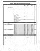
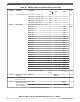
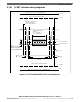
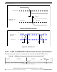
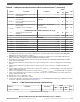
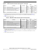
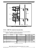

Table 20. LVDS pad startup and receiver electrical characteristics
1
(continued)
Symbol Parameter Conditions
Value
Unit
Min Typ Max
t
PD2NM_TX
Transmitter startup time (power down to
Normal mode)
5
— — 0.4 2.75 μs
t
SM2NM_TX
Transmitter startup time (Sleep mode to
Normal mode)
6
Not applicable to the MSC/DSPI
LVDS pad
— 0.2 0.5 μs
t
PD2NM_RX
Receiver startup time (power down to
Normal mode)
7
— — 20 40 ns
t
PD2SM_RX
Receiver startup time (power down to
Sleep mode)
8
Not applicable to the MSC/DSPI
LVDS pad
— 20 50 ns
I
LVDS_BIAS
LVDS bias current consumption Tx or Rx enabled — — 0.95 mA
TRANSMISSION LINE CHARACTERISTICS (PCB Track)
Z
0
Transmission line characteristic
impedance
— 47.5 50 52.5 Ω
Z
DIFF
Transmission line differential impedance — 95 100 105 Ω
RECEIVER
V
ICOM
Common mode voltage — 0.15
9
— 1.6
10
V
|ΔVI| Differential input voltage — 100 — — mV
V
HYS
Input hysteresis — 25 — — mV
R
IN
Terminating resistance V
DDEH
= 3.0 V to 5.5 V 80 125 150 Ω
C
IN
Differential input capacitance
11
— — 3.5 6.0 pF
I
LVDS_RX
Receiver DC current consumption Enabled — — 0.5 mA
1. The LVDS pad startup and receiver electrical characteristics in this table apply to both the LFAST and the MSC/DSPI
LVDS pad except where noted in the conditions.
2. All startup times are defined after a 2 peripheral bridge clock delay from writing to the corresponding enable bit in the
LVDS control registers (LCR) of the LFAST and High-Speed Debug modules.
3. Startup times are valid for the maximum external loads CL defined in both the LFAST/HSD and MSC/DSPI transmitter
electrical characteristic tables.
4. Bias startup time is defined as the time taken by the current reference block to reach the settling bias current after being
enabled.
5. Total transmitter startup time from power down to normal mode is t
STRT_BIAS
+ t
PD2NM_TX
+ 2 peripheral bridge clock
periods.
6. Total transmitter startup time from sleep mode to normal mode is t
SM2NM_TX
+ 2 peripheral bridge clock periods. Bias block
remains enabled in sleep mode.
7. Total receiver startup time from power down to normal mode is t
STRT_BIAS
+ t
PD2NM_RX
+ 2 peripheral bridge clock periods.
8. Total receiver startup time from power down to sleep mode is t
PD2SM_RX
+ 2 peripheral bridge clock periods. Bias block
remains enabled in sleep mode.
9. Absolute min = 0.15 V – (285 mV/2) = 0 V
10. Absolute max = 1.6 V + (285 mV/2) = 1.743 V
11. Total internal capacitance including receiver and termination, co-bonded GPIO pads, and package contributions. For bare
die devices, subtract the package value given in Figure 11.
Table 21. LFAST transmitter electrical characteristics
1
Symbol Parameter Conditions
Value
Unit
Min Typ Max
f
DATA
Data rate — — — 240 Mbps
Table continues on the next page...
Electrical characteristics
MPC5777C Microcontroller Data Sheet Data Sheet, Rev. 13, 08/2018.
NXP Semiconductors 37