
Datasheet
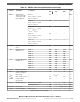
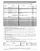
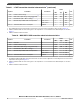

Table 18. SDADC electrical specifications (continued)
Symbol Parameter Conditions
Value
Unit
Min Typ Max
t
SETTLING
Settling time after mux
change
Analog inputs are muxed
HPF = ON
— — 2*δ
GROUP
+
3*f
ADCD_S
—
HPF = OFF — — 2*δ
GROUP
+
2*f
ADCD_S
t
ODRECOVERY
Overdrive recovery
time
After input comes within range from
saturation
HPF = ON
— — 2*δ
GROUP
+
f
ADCD_S
—
HPF = OFF — — 2*δ
GROUP
C
S_D
SDADC sampling
capacitance after
sampling switch
16
GAIN = 1, 2, 4, 8 — — 75*GAIN fF
GAIN = 16 — — 600 fF
I
BIAS
Bias consumption At least one SDADC enabled — — 3.5 mA
I
ADV_D
SDADC supply
consumption
Per SDADC enabled — — 4.325 mA
I
ADR_D
SDADC reference
current consumption
Per SDADC enabled — — 20 μA
1. For input voltage above the maximum and below the clamp voltage of the input pad, there is no latch-up concern, and the
signal will only be “clipped.”
2. VINP is the input voltage applied to the positive terminal of the SDADC
3. VINM is the input voltage applied to the negative terminal of the SDADC
4. Sampling is generated internally f
SAMPLING
= f
ADCD_M
/2
5. For Gain = 16, SDADC resolution is 15 bit.
6. Calibration of gain is possible when gain = 1. Offset Calibration should be done with respect to 0.5*V
RH_SD
for differential
mode and single ended mode with negative input = 0.5*V
RH_SD
. Offset Calibration should be done with respect to 0 for
single ended mode with negative input = 0. Both Offset and Gain Calibration is guaranteed for +/–5% variation of V
RH_SD
,
+/–10% variation of V
DDA_SD
, +/–50 C temperature variation.
7. Offset and gain error due to temperature drift can occur in either direction (+/–) for each of the SDADCs on the device.
8. SDADC is functional in the range 3.6 V < V
DDA_SD
< 4.0 V: SNR parameter degrades by 3 dB. SDADC is functional in the
range 3.0 V < V
RH_SD
< 4.0 V: SNR parameter degrades by 9 dB.
9. SNR values guaranteed only if external noise on the ADC input pin is attenuated by the required SNR value in the
frequency range of f
ADCD_M
– f
ADCD_S
to f
ADCD_M
+ f
ADCD_S
, where f
ADCD_M
is the input sampling frequency and f
ADCD_S
is
the output sample frequency. A proper external input filter should be used to remove any interfering signals in this
frequency range.
10. Input impedance in differential mode Z
IN
= Z
DIFF
11. Input impedance given at f
ADCD_M
= 16 MHz. Impedance is inversely proportional to SDADC clock frequency. Z
DIFF
(f
ADCD_M
) = (16 MHz / f
ADCD_M
) * Z
DIFF
, Z
CM
(f
ADCD_M
) = (16 MHz / f
ADCD_M
) * Z
CM
.
12. Input impedance in single-ended mode Z
IN
= (2 * Z
DIFF
* Z
CM
) / (Z
DIFF
+ Z
CM
)
13. V
INTCM
is the Common Mode input reference voltage for the SDADC. It has a nominal value of (V
RH_SD
- V
RL_SD
) / 2.
14. The ±1% passband ripple specification is equivalent to 20 * log
10
(0.99) = 0.087 dB.
15. Propagation of the information from the pin to the register CDR[CDATA] and the flags SFR[DFEF] and SFR[DFFF] is
given by the different modules that must be crossed: delta/sigma filters, high pass filter, FIFO module, and clock domain
synchronizers. The time elapsed between data availability at the pin and internal SDADC module registers is given by the
following formula, where f
ADCD_S
is the frequency of the sampling clock, f
ADCD_M
is the frequency of the modulator, and
f
FM_PER_CLK
is the frequency of the peripheral bridge clock feeds to the SDADC module:
REGISTER LATENCY = t
LATENCY
+ 0.5/f
ADCD_S
+ 2 (~+1)/f
ADCD_M
+ 2(~+1)f
FM_PER_CLK
The (~+1) symbol refers to the number of clock cycles uncertainty (from 0 to 1 clock cycle) to be added due to
resynchronization of the signal during clock domain crossing.
Electrical characteristics
MPC5777C Microcontroller Data Sheet Data Sheet, Rev. 13, 08/2018.
NXP Semiconductors 33