
Datasheet

1 Introduction
1.1 Features summary
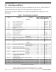
On-chip modules available within the family include the following features:
• Three dual issue, 32-bit CPU core complexes (e200z7), two of which run in lockstep
• Power Architecture embedded specification compliance
• Instruction set enhancement allowing variable length encoding (VLE), optional
encoding of mixed 16-bit and 32-bit instructions, for code size footprint
reduction
• On the two computational cores: Signal processing extension (SPE1.1)
instruction support for digital signal processing (DSP)
• Single-precision floating point operations
• On the two computational cores: 16 KB I-Cache and 16 KB D-Cache
• Hardware cache coherency between cores
• 16 hardware semaphores
• 3-channel CRC module
• 8 MB on-chip flash memory
• Supports read during program and erase operations, and multiple blocks
allowing EEPROM emulation
• 512 KB on-chip general-purpose SRAM including 64 KB standby RAM
• Two multichannel direct memory access controllers (eDMA)
• 64 channels per eDMA
• Dual core Interrupt Controller (INTC)
• Dual phase-locked loops (PLLs) with stable clock domain for peripherals and
frequency modulation (FM) domain for computational shell
• Crossbar Switch architecture for concurrent access to peripherals, flash memory, or
RAM from multiple bus masters with End-To-End ECC
• External Bus Interface (EBI) for calibration and application use
• System Integration Unit (SIU)
• Error Injection Module (EIM) and Error Reporting Module (ERM)
• Four protected port output (PPO) pins
• Boot Assist Module (BAM) supports serial bootload via CAN or SCI
• Three second-generation Enhanced Time Processor Units (eTPUs)
• 32 channels per eTPU
• Total of 36 KB code RAM
• Total of 9 KB parameter RAM
Introduction
MPC5777C Microcontroller Data Sheet Data Sheet, Rev. 13, 08/2018.
NXP Semiconductors 3