
Datasheet

5. At V
RH_EQ
– V
RL_EQ
= 5.12 V, one LSB = 1.25 mV.
6. Below disruptive current conditions, the channel being stressed has conversion values of $3FF for analog inputs greater
than V
RH
and $000 for values less than V
RL
. Other channels are not affected by non-disruptive conditions.
7. Exceeding limit may cause conversion error on stressed channels and on unstressed channels. Transitions within the limit
do not affect device reliability or cause permanent damage.
8. Input must be current limited to the value specified. To determine the value of the required current-limiting resistor,
calculate resistance values using V
POSCLAMP
= V
DDA
+ 0.5 V and V
NEGCLAMP
= –0.3 V, then use the larger of the calculated
values.
9. Condition applies to two adjacent pins at injection limits.
10. Performance expected with production silicon.
11. All channels have same 10 kΩ < Rs < 100 kΩ Channel under test has Rs = 10 kΩ, I
INJ
=I
INJMAX
,I
INJMIN
.
12. The TUE specification is always less than the sum of the INL, DNL, offset, and gain errors due to cancelling errors.
13. TUE does not apply to differential conversions.
14. Variable gain is controlled by setting the PRE_GAIN bits in the ADC_ACR1-8 registers to select a gain factor of ×1, ×2, or
×4. Settings are for differential input only. Tested at ×1 gain. Values for other settings are guaranteed as indicated.
15. Guaranteed 10-bit monotonicity.
16. At V
RH_EQ
– V
RL_EQ
= 5.12 V, one LSB = 1.25 mV.
3.8.2 Sigma-Delta ADC (SDADC)
The SDADC is a 16-bit Sigma-Delta analog-to-digital converter with a 333 Ksps
maximum output conversion rate.
NOTE
The voltage range is 4.5 V to 5.5 V for SDADC specifications,
except where noted otherwise.
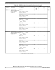
Table 18. SDADC electrical specifications
Symbol Parameter Conditions
Value
Unit
Min Typ Max
V
IN
ADC input signal — 0 — V
DDA_SD
V
V
IN_PK2PK
1
Input range peak to
peak
V
IN_PK2PK
= V
INP
2
–
V
INM
, 3
Single ended
V
INM
= V
RL_SD
V
RH_SD
/GAIN V
Single ended
V
INM
= 0.5*V
RH_SD
GAIN = 1
±0.5*V
RH_SD
Single ended
V
INM
= 0.5*V
RH_SD
GAIN = 2,4,8,16
±V
RH_SD
/GAIN
Differential
0 < V
IN
< V
DDEx
±V
RH_SD
/GAIN
f
ADCD_M
SD clock frequency
4
— 4 14.4 16 MHz
f
ADCD_S
Conversion rate — — — 333 Ksps
— Oversampling ratio Internal modulator 24 — 256 —
RESOLUTION SD register resolution
5
2's complement notation 16 bit
Table continues on the next page...
Electrical characteristics
MPC5777C Microcontroller Data Sheet Data Sheet, Rev. 13, 08/2018.
NXP Semiconductors 25