
Datasheet

3.7 Oscillator and PLL electrical specifications
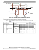
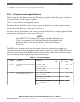
The on-chip dual PLL—consisting of the peripheral clock and reference PLL (PLL0) and
the frequency-modulated system PLL (PLL1)—generates the system and auxiliary clocks
from the main oscillator driver.
IRC
XOSC
PLL0
PLL0_PHI
PLL0_PHI1
PLL1_PHI
PLL1
Figure 6. PLL integration
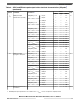
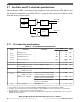
3.7.1 PLL electrical specifications
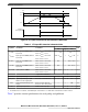
Table 12. PLL0 electrical characteristics
Symbol Parameter Conditions
Value
Unit
Min Typ Max
f
PLL0IN
PLL0 input clock
1, 2
— 8 — 44 MHz
Δ
PLL0IN
PLL0 input clock duty cycle
2
— 40 — 60 %
f
PLL0VCO
PLL0 VCO frequency — 600 — 1250 MHz
f
PLL0PHI
PLL0 output frequency — 4.762 — 200/24
0
3
MHz
t
PLL0LOCK
PLL0 lock time — — — 110 μs
|Δ
PLL0PHISPJ
| PLL0_PHI single period jitter
f
PLL0IN
= 20 MHz (resonator)
f
PLL0PHI
= 200 MHz, 6-sigma — — 200 ps
|Δ
PLL0PHI1SPJ
| PLL0_PHI1 single period jitter
f
PLL0IN
= 20 MHz (resonator)
f
PLL0PHI1
= 40 MHz, 6-sigma — — 300
4
ps
Δ
PLL0LTJ
PLL0 output long term jitter
4
f
PLL0IN
= 20 MHz (resonator),
VCO frequency = 800 MHz
10 periods accumulated jitter (80 MHz
equivalent frequency), 6-sigma pk-pk
— — ±250 ps
16 periods accumulated jitter (50 MHz
equivalent frequency), 6-sigma pk-pk
— — ±300 ps
long term jitter (< 1 MHz equivalent
frequency), 6-sigma pk-pk)
— — ±500 ps
I
PLL0
PLL0 consumption FINE LOCK state — — 7.5 mA
1. Ensure that the f
PLL0IN
frequency divided by PLLDIG_PLL0DV[PREDIV] is in the range 8 MHz to 20 MHz.
2. PLL0IN clock retrieved directly from either internal IRC or external XOSC clock. Input characteristics are granted when
using internal IRC or external oscillator is used in functional mode.
3. 200 MHz applies to the MPC5777C part number with 264 MHz operating frequency. 240 MHz applies to the version with
300 MHz operating frequency
Electrical characteristics
MPC5777C Microcontroller Data Sheet Data Sheet, Rev. 13, 08/2018.
20 NXP Semiconductors