
Datasheet

1. PCR[DSC] values refer to the setting of that register field in the SIU.
3.6.3 I/O pad current specifications
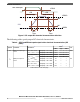
The I/O pads are distributed across the I/O supply segments. Each I/O supply segment is
associated with a V
DDEx
supply segment.
Table 11 provides I/O consumption figures.
To ensure device reliability, the average current of the I/O on a single segment should
remain below the I
MAXSEG
value given in Table 1.
To ensure device functionality, the average current of the I/O on a single segment should
remain below the I
MAXSEG
value given in Table 3.
NOTE
The MPC5777C I/O Signal Description and Input Multiplexing
Tables are contained in a Microsoft Excel® file attached to the
Reference Manual. In the spreadsheet, select the I/O Signal
Table tab.
The EBI power segments have been designed to operate within the maximum per-
segment current specification when the pins on the segment are used for EBI function. If
the pins are used instead for GPIO function, the user must ensure the sum of the current
used on each pin in the segment does not exceed the spec.
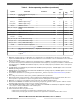
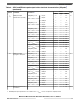
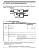
Table 11. I/O consumption
Symbol Parameter Conditions
Value
Unit
Min Typ Max
I
AVG_GPIO
Average I/O current for GPIO pads
(per pad)
C
L
= 25 pF, 2 MHz
V
DDEx
= 5.0 V ± 10%
— — 0.42 mA
C
L
= 50 pF, 1 MHz
V
DDEx
= 5.0 V ± 10%
— — 0.35
I
AVG_EBI
Average I/O current for external
bus output pins (per pad)
C
DRV
= 10 pF, f
EBI
= 66 MHz
V
DDEx
= 3.3 V ± 10%
— — 9 mA
C
DRV
= 20 pF, f
EBI
= 66 MHz
V
DDEx
= 3.3 V ± 10%
— — 18
C
DRV
= 30 pF, f
EBI
= 66 MHz
V
DDEx
= 3.3 V ± 10%
— — 30
Electrical characteristics
MPC5777C Microcontroller Data Sheet Data Sheet, Rev. 13, 08/2018.
NXP Semiconductors 19