
Datasheet

2. PCR[SRC] values refer to the setting of that register field in the SIU.
3. All values to be confirmed during device validation.
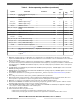
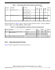
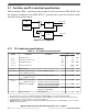
The following table shows the EBI CLKOUT, address, and control signal pad electrical
characteristics. These pads can also be used for GPIO.
Table 10. GPIO and EBI CLKOUT, address, and control signal pad output
buffer electrical characteristics (FC pads)
Symbol Parameter Conditions
1
Value
Unit
Min Typ Max
EBI Mode Output Specifications: valid for 3.0 V < V
DDEx
< 3.6 V
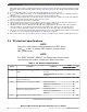
C
DRV
External bus load
capacitance
PCR[DSC] = 01b — — 10 pF
PCR[DSC] = 10b — — 20
PCR[DSC] = 11b — — 30
f
MAX_EBI
External bus maximum
operating frequency
C
DRV
= 10/20/30 pF — — 66 MHz
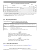
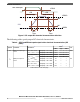
GPIO and EBI Mode Output Specifications
I
OH_EBI
GPIO and external bus
pad output high current
V
OH
= 0.8 * V
DDEx
4.5 V < V
DDEx
< 5.5 V
PCR[DSC] = 11b 30 — — mA
PCR[DSC] = 10b 22 — —
PCR[DSC] = 01b 13 — —
PCR[DSC] = 00b 2 — —
V
OH
= 0.8 * V
DDEx
3.0 V < V
DDEx
< 3.6 V
PCR[DSC] = 11b 16 — —
PCR[DSC] = 10b 12 — —
PCR[DSC] = 01b 7 — —
PCR[DSC] = 00b 1 — —
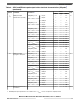
I
OL_EBI
GPIO and external bus
pad output low current
V
OL
= 0.2 * V
DDEx
4.5 V < V
DDEx
< 5.5 V
PCR[DSC] = 11b 54 — — mA
PCR[DSC] = 10b 25 — —
PCR[DSC] = 01b 16 — —
PCR[DSC] = 00b 2 — —
V
OL
= 0.2 * V
DDEx
3.0 V < V
DDEx
< 3.6 V
PCR[DSC] = 11b 17 — —
PCR[DSC] = 10b 14 — —
PCR[DSC] = 01b 8 — —
PCR[DSC] = 00b 1 — —
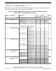
t
R_F_EBI
GPIO and external bus
pad output transition
time (rise/fall)
PCR[DSC] = 11b C
L
= 30 pF — — 1.5 ns
C
L
= 50 pF — — 2.4
PCR[DSC] = 10b C
L
= 20 pF — — 1.5
PCR[DSC] = 01b C
L
= 10 pF — — 1.85
PCR[DSC] = 00b C
L
= 50 pF — — 45
t
PD_EBI
GPIO and external bus
pad output propagation
delay time
PCR[DSC] = 11b C
L
= 30 pF — — 4.2 ns
C
L
= 50 pF — — 5.5
PCR[DSC] = 10b C
L
= 20 pF — — 4.2
PCR[DSC] = 01b C
L
= 10 pF — — 4.4
PCR[DSC] = 00b C
L
= 50 pF — — 59
Electrical characteristics
MPC5777C Microcontroller Data Sheet Data Sheet, Rev. 13, 08/2018.
18 NXP Semiconductors