
Datasheet
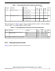
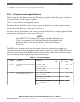

core side input
PAD
Voh
Vol
tPD
(low to high)
Fall
Time
VDDEx
VSSEx
Rise
Time
tPD
(high to low)
VDD/2
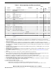
Figure 5. I/O output DC electrical characteristics definition
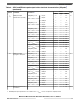
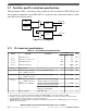
The following tables specify output DC electrical characteristics.
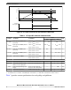
Table 9. GPIO and EBI data pad output buffer electrical characteristics (SR
pads)
1
Symbol Parameter Conditions
2
Value
3
Unit
Min Typ Max
I
OH
GPIO pad output high
current
V
OH
= 0.8 * V
DDEx
4.5 V < V
DDEx
< 5.5 V
PCR[SRC] = 11b or 01b 25 — — mA
PCR[SRC] = 10b or 00b 15 — —
V
OH
= 0.8 * V
DDEx
3.0 V < V
DDEx
< 3.6 V
PCR[SRC] = 11b or 01b 13 — —
PCR[SRC] = 10b or 00b 8 — —
I
OL
GPIO pad output low
current
V
OL
= 0.2 * V
DDEx
4.5 V < V
DDEx
< 5.5 V
PCR[SRC] = 11b or 01b 48 — — mA
PCR[SRC] = 10b or 00b 22 — —
V
OL
= 0.2 * V
DDEx
3.0 V < V
DDEx
< 3.6 V
PCR[SRC] = 11b or 01b 17 — —
PCR[SRC] = 10b or 00b 10.5 — —
Table continues on the next page...
Electrical characteristics
MPC5777C Microcontroller Data Sheet Data Sheet, Rev. 13, 08/2018.
16 NXP Semiconductors