
Datasheet
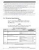
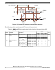
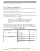

V IN
V INTERNAL
(SIU register)
V DD
V IH
V HYS
V IL
Figure 4. I/O input DC electrical characteristics definition
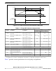
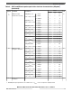
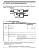
Table 6. I/O input DC electrical characteristics
Symbol Parameter Conditions
Value
Unit
Min Typ Max
V
IHCMOS_H
Input high level CMOS (with
hysteresis)
3.0 V < V
DDEx
< 3.6 V and
4.5 V < V
DDEx
< 5.5 V
0.65 * V
DDEx
— V
DDEx
+ 0.3 V
V
IHCMOS
Input high level CMOS (without
hysteresis)
3.0 V < V
DDEx
< 3.6 V and
4.5 V < V
DDEx
< 5.5 V
0.55 * V
DDEx
— V
DDEx
+ 0.3 V
V
ILCMOS_H
Input low level CMOS (with
hysteresis)
3.0 V < V
DDEx
< 3.6 V and
4.5 V < V
DDEx
< 5.5 V
–0.3 — 0.35 * V
DDEx
V
V
ILCMOS
Input low level CMOS (without
hysteresis)
3.0 V < V
DDEx
< 3.6 V and
4.5 V < V
DDEx
< 5.5 V
–0.3 — 0.4 * V
DDEx
V
V
HYSCMOS
Input hysteresis CMOS 3.0 V < V
DDEx
< 3.6 V and
4.5 V < V
DDEx
< 5.5 V
0.1 * V
DDEx
— — V
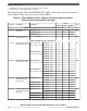
Input Characteristics
1
I
LKG
Digital input leakage V
SS
< V
IN
< V
DDEx
/V
DDEHx
— — 2.5 μA
I
LKG_FAST
Digital input leakage for EBI
address/control signal pads
V
SS
< V
IN
< V
DDEx
/V
DDEHx
— — 2.5 μA
I
LKGA
Analog pin input leakage (5 V
range)
V
SSA_SD
< V
IN
< V
DDA_SD
,
V
SSA_EQ
< V
IN
< V
DDA_EQA/B
— — 220 nA
C
IN
Digital input capacitance GPIO and EBI input pins — — 7 pF
1. For LFAST, microsecond bus, and LVDS input characteristics, see dedicated communication module sections.
Table 7 provides current specifications for weak pullup and pulldown.
Electrical characteristics
MPC5777C Microcontroller Data Sheet Data Sheet, Rev. 13, 08/2018.
14 NXP Semiconductors