
Datasheet
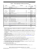
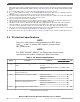
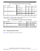
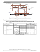
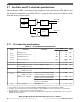

Table 4. DC electrical specifications (continued)
Symbol Parameter Conditions
Value
Unit
Min Typ Max
I
STBY
Standby RAM supply current (T
J
= 150°C) 1.08 V — — 1140 μA
1.25 V to 5.5 V — — 1170
I
DD_PWR
Operating current on the V
DDPWR
supply — — — 50 mA
I
BG_REF
Bandgap reference current consumption
3
— — 600 μA
I
TRNG
True Random Number Generator current — — — 2.1 mA
1. I
DD
measured on an application-specific pattern with all cores enabled at full frequency, T
J
= 40°C to 150°C. Flash memory
program/erase current on the V
DD
supply not included.
2. This value is considering the use of the internal core regulator with the simulation of an external transistor with the
minimum value of h
FE
of 60.
3. This bandgap reference is for EQADC calibration and Temperature Sensors.
3.6 I/O pad specifications
The following table describes the different pad types on the chip.
Table 5. I/O pad specification descriptions
Pad type Description
General-purpose I/O
pads
General-purpose I/O and EBI data bus pads with four selectable output slew rate settings; also
called SR pads
EBI pads Provide necessary speed for fast external memory interfaces on the EBI CLKOUT, address, and
control signals; also called FC pads
LVDS pads Low Voltage Differential Signal interface pads
Input-only pads Low-input-leakage pads that are associated with the ADC channels
NOTE
Each I/O pin on the device supports specific drive
configurations. See the signal description table in the device
reference manual for the available drive configurations for each
I/O pin.
NOTE
Throughout the I/O pad specifications, the symbol V
DDEx
represents all V
DDEx
and V
DDEHx
segments.
3.6.1 Input pad specifications
Table 6 provides input DC electrical characteristics as described in Figure 4.
Electrical characteristics
MPC5777C Microcontroller Data Sheet Data Sheet, Rev. 13, 08/2018.
NXP Semiconductors 13