
Datasheet

When flash memory power is supplied externally (V
DDPMC
shorted to V
DDFLA
): The V
DDPMC
range must be within the limits
specified for LVD_FLASH and HVD_FLASH monitoring. Table 29 provides the monitored LVD_FLASH and HVD_FLASH
limits.
13. If the standby RAM regulator is not used, the V
STBY
supply input pin must be tied to ground.
14. V
STBY_BO
is the maximum voltage that sets the standby RAM brownout flag in the device logic. The minimum voltage for
RAM data retention is guaranteed always to be less than the V
STBY_BO
maximum value.
15. For supply voltages between 3.0 V and 4.0 V there will be no guaranteed precision of ADC (accuracy/linearity). ADC will
recover to a fully functional state when the voltage rises above 4.0 V.
16. Full device lifetime without performance degradation
17. I/O and analog input specifications are only valid if the injection current on adjacent pins is within these limits. See the
absolute maximum ratings table for maximum input current for reliability requirements.
18. The I/O pins on the device are clamped to the I/O supply rails for ESD protection. When the voltage of the input pin is
above the supply rail, current will be injected through the clamp diode to the supply rail. For external RC network
calculation, assume a typical 0.3 V drop across the active diode. The diode voltage drop varies with temperature.
19. The sum of all controller pins (including both digital and analog) must not exceed 200 mA. A V
DDEx
/V
DDEHx
power segment
is defined as one or more GPIO pins located between two V
DDEx
/V
DDEHx
supply pins.
20. The average current values given in I/O pad current specifications should be used to calculate total I/O segment current.
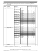
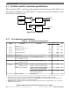
3.5 DC electrical specifications
NOTE
I
DDA_MISC
is the sum of current consumption of IRC, I
TRNG
,
and I
STBY
in the 5 V domain. IRC current is provided in the
IRC specifications.
NOTE
I/O, XOSC, EQADC, SDADC, and Temperature Sensor current
specifications are in those components' dedicated sections.
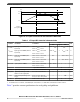
Table 4. DC electrical specifications
Symbol Parameter Conditions
Value
Unit
Min Typ Max
I
DD
Operating current on the V
DD
core logic
supply
1
LVD/HVD enabled, V
DD
= 1.2 V
to 1.32 V
— 0.65 1.35 A
LVD/HVD disabled, V
DD
= 1.2 V
to 1.38 V
— 0.65 1.4
I
DD_PE
Operating current on the V
DD
supply for flash
memory program/erase
— — — 85 mA
I
DDPMC
Operating current on the V
DDPMC
supply
2
Flash memory read — — 40 mA
Flash memory program/erase — — 70
PMC only — — 35
Operating current on the V
DDPMC
supply
(internal core regulator bypassed)
Flash memory read — — 10 mA
Flash memory program/erase — — 40
PMC only — — 5
I
REGCTL
Core regulator DC current output on V
REGCTL
pin
— — — 25 mA
Table continues on the next page...
Electrical characteristics
MPC5777C Microcontroller Data Sheet Data Sheet, Rev. 13, 08/2018.
12 NXP Semiconductors