
Datasheet
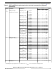
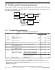

Table 3. Device operating conditions (continued)
Symbol Parameter Conditions
Value
Unit
Min Typ Max
V
STBY_BO
Standby RAM brownout flag trip
point voltage
— — — 0.9
14
V
V
RL_SD
SDADC ground reference
voltage
—
V
SSA_SD
V
V
DDA_SD
SDADC supply voltage
15
— 4.5 — 5.5 V
V
DDA_EQA/B
eQADC supply voltage — 4.75 — 5.25 V
V
RH_SD
SDADC reference — 4.5 V
DDA_SD
5.5 V
V
DDA_SD
– V
RH_SD
SDADC reference differential
voltage
— — — 25 mV
V
SSA_SD
– V
RL_SD
V
RL_SD
differential voltage — –25 — 25 mV
V
RH_EQ
eQADC reference — 4.75 — 5.25 V
V
DDA_EQA/B
–
V
RH_EQ
eQADC reference differential
voltage
— — — 25 mV
V
SSA_EQ
– V
RL_EQ
V
RL_EQ
differential voltage — –25 — 25 mV
V
SSA_EQ
– V
SS
V
SSA_EQ
differential voltage — –25 — 25 mV
V
SSA_SD
– V
SS
V
SSA_SD
differential voltage — –25 — 25 mV
V
RAMP
Slew rate on power supply pins — — — 100 V/ms
Current
I
IC
DC injection current (per pin)
16,
17, 18
Digital pins and analog pins –3.0 — 3.0 mA
I
MAXSEG
Maximum current per power
segment
19, 20
— –80 — 80 mA
1. Maximum operating frequency is applicable to the computational cores and platform for the device. See the Clocking
chapter in the MPC5777C Microcontroller Reference Manual for more information on the clock limitations for the various IP
blocks on the device.
2. If frequency modulation (FM) is enabled for the operating frequency of 264MHz, the maximum frequency still cannot
exceed this value (frequency modulation must spread below nominal frequency). If frequency modulation is enabled for the
operating frequency of 300MHz, this maximum frequency can be exceeded (frequency modulation can be center spread
from 300MHz).
3. 132 MHz applies to the MPC5777C part number with 264 MHz operating frequency. 150 MHz applies to the version with
300 MHz operating frequency.
4. 200 MHz applies to the MPC5777C part number with 264 MHz max operating frequency. 240 MHz applies to the version
with 300 MHz operating frequency.
5. The maximum specification for operating junction temperature T
J
must be respected. Thermal characteristics provides
details.
6. Core voltage as measured on device pin to guarantee published silicon performance
7. During power ramp, voltage measured on silicon might be lower. Maximum performance is not guaranteed, but correct
silicon operation is guaranteed. See power management and reset management for description.
8. Maximum core voltage is not permitted for entire product life. See absolute maximum rating.
9. When internal LVD/HVDs are disabled, external monitoring is required to guarantee device operation. Failure to monitor
externally supply voltage may result in erroneous operation of the device.
10. This LVD/HVD disabled supply voltage condition only applies after LVD/HVD are disabled by the application during the
reset sequence, and the LVD/HVD are active until that point.
11. This spec does not apply to V
DDEH1
.
12. When internal flash memory regulator is used:
•
Flash memory read operation is supported for a minimum V
DDPMC
value of 3.15 V.
• Flash memory read, program, and erase operations are supported for a minimum V
DDPMC
value of 3.5 V.
Electrical characteristics
MPC5777C Microcontroller Data Sheet Data Sheet, Rev. 13, 08/2018.
NXP Semiconductors 11