NXP Semiconductors Data Sheet: Technical Data Document Number: MPC5777C Rev. 13, 08/2018 MPC5777C MPC5777C Microcontroller Data Sheet Features • This document provides electrical specifications, pin assignments, and package diagram information for the MPC5777C series of microcontroller units (MCUs). • For functional characteristics and the programming model, see the MPC5777C Reference Manual.
Table of Contents 1 Introduction...............................................................................3 3.11.1 Power management electrical characteristics40 1.1 Features summary..........................................................3 3.11.2 Power management integration.....................43 1.2 Block diagram..................................................................4 3.11.3 Device voltage monitoring..............................44 2 Pinouts.....................................
Introduction 1 Introduction 1.1 Features summary On-chip modules available within the family include the following features: • Three dual issue, 32-bit CPU core complexes (e200z7), two of which run in lockstep • Power Architecture embedded specification compliance • Instruction set enhancement allowing variable length encoding (VLE), optional encoding of mixed 16-bit and 32-bit instructions, for code size footprint reduction • On the two computational cores: Signal processing extension (SPE1.
Introduction • Enhanced Modular Input/Output System (eMIOS) supporting 32 unified channels with each channel capable of single action, double action, pulse width modulation (PWM) and modulus counter operation • Two Enhanced Queued Analog-to-Digital Converter (eQADC) modules with: • Two separate analog converters per eQADC module • Support for a total of 70 analog input pins, expandable to 182 inputs with offchip multiplexers • Interface to twelve hardware Decimation Filters • Enhanced "Tap" command to rout
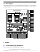
Pinouts 1.2 Block diagram The following figure shows a top-level block diagram of the MPC5777C. The purpose of the block diagram is to show the general interconnection of functional modules through the crossbar switch.
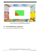
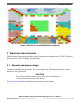
Pinouts Figure 2. MPC5777C 416-ball MAPBGA (full diagram) 2.2 516-ball MAPBGA pin assignments Figure 3 shows the 516-ball MAPBGA pin assignments. MPC5777C Microcontroller Data Sheet Data Sheet, Rev. 13, 08/2018.
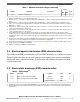
Electrical characteristics Figure 3. MPC5777C 516-ball MAPBGA (full diagram) 3 Electrical characteristics The following information includes details about power considerations, DC/AC electrical characteristics, and AC timing specifications. 3.1 Absolute maximum ratings Absolute maximum specifications are stress ratings only. Functional operation at these maxima is not guaranteed. CAUTION Stress beyond listed maxima may affect device reliability or cause permanent damage to the device.
Electrical characteristics Table 1. Absolute maximum ratings Symbol Cycle VDD VDDEHx VDDEx Conditions1 Parameter Lifetime power cycles 1.2 V core supply voltage2, 3, 4 I/O supply voltage (medium I/O I/O supply voltage (fast I/O pads)5 pads)5 Value Unit Min Max — — 1000k — — –0.3 1.5 V — –0.3 6.0 V — –0.3 6.0 V VDDPMC Power Management Controller supply voltage5 — –0.3 6.0 V VDDFLA Decoupling pin for flash regulator6 — –0.3 4.
Electrical characteristics Table 1. Absolute maximum ratings (continued) Symbol Moisture sensitivity level11 MSL Value Conditions1 Parameter Min Max — 3 — Unit — 1. Voltages are referred to VSS if not specified otherwise 2. Allowed 1.45 V – 1.5 V for 60 seconds cumulative time at maximum TJ = 150 °C; remaining time as defined in note 3 and note 4 3. Allowed 1.375 V – 1.45 V for 10 hours cumulative time at maximum TJ = 150 °C; remaining time as defined in note 4 4. 1.32 V – 1.
Electrical characteristics 3.4 Operating conditions The following table describes the operating conditions for the device, and for which all specifications in the data sheet are valid, except where explicitly noted. If the device operating conditions are exceeded, the functionality of the device is not guaranteed. Table 3.
Electrical characteristics Table 3. Device operating conditions (continued) Symbol VSTBY_BO Parameter Conditions Value Min Typ Max — — 0.914 Standby RAM brownout flag trip point voltage — VRL_SD SDADC ground reference voltage — VDDA_SD SDADC supply voltage15 — 4.5 eQADC supply voltage — SDADC reference — VDDA_SD – VRH_SD SDADC reference differential voltage VSSA_SD – VRL_SD Unit V V VSSA_SD — 5.5 V 4.75 — 5.25 V 4.5 VDDA_SD 5.
Electrical characteristics 13. 14. 15. 16. 17. 18. 19. 20. When flash memory power is supplied externally (VDDPMC shorted to VDDFLA): The VDDPMC range must be within the limits specified for LVD_FLASH and HVD_FLASH monitoring. Table 29 provides the monitored LVD_FLASH and HVD_FLASH limits. If the standby RAM regulator is not used, the VSTBY supply input pin must be tied to ground. VSTBY_BO is the maximum voltage that sets the standby RAM brownout flag in the device logic.
Electrical characteristics Table 4. DC electrical specifications (continued) Symbol ISTBY IDD_PWR IBG_REF ITRNG Parameter Standby RAM supply current (TJ = 150°C) Operating current on the VDDPWR supply Bandgap reference current Conditions Unit Min Typ Max 1.08 V — — 1140 1.25 V to 5.5 V — — 1170 — — — 50 mA — — 600 μA — — 2.1 mA consumption3 True Random Number Generator current Value — μA 1.
Electrical characteristics V IN V DD V IH V HYS V IL V INTERNAL (SIU register) Figure 4. I/O input DC electrical characteristics definition Table 6. I/O input DC electrical characteristics Symbol VIHCMOS_H VIHCMOS VILCMOS_H VILCMOS VHYSCMOS Parameter Conditions Input high level CMOS (with hysteresis) 3.0 V < VDDEx < 3.6 V and Input high level CMOS (without hysteresis) 3.0 V < VDDEx < 3.6 V and Input low level CMOS (with hysteresis) 3.0 V < VDDEx < 3.
Electrical characteristics Table 7. I/O pullup/pulldown DC electrical characteristics Symbol IWPU Parameter Conditions Weak pullup current VIN = 0.35 * VDDEx Value Min Typ Max 40 — 120 25 — 80 40 — 120 25 — 80 Unit μA 4.5 V < VDDEx < 5.5 V VIN = 0.35 * VDDEx 3.0 V < VDDEx < 3.6 V IWPD Weak pulldown current VIN = 0.65 * VDDEx μA 4.5 V < VDDEx < 5.5 V VIN = 0.65 * VDDEx 3.0 V < VDDEx < 3.
Electrical characteristics core side input VDD/2 tPD (low to high) tPD (high to low) VDDEx Voh PAD Vol VSSEx Rise Time Fall Time Figure 5. I/O output DC electrical characteristics definition The following tables specify output DC electrical characteristics. Table 9. GPIO and EBI data pad output buffer electrical characteristics (SR pads)1 Symbol IOH IOL Parameter Conditions2 GPIO pad output high current VOH = 0.
Electrical characteristics Table 9. GPIO and EBI data pad output buffer electrical characteristics (SR pads)1 (continued) Symbol tR_F Parameter Conditions2 GPIO pad output transition time (rise/fall) PCR[SRC] = 11b Min Typ Max CL = 25 pF — — 1.2 4.5 V < VDDEx < 5.5 V CL = 50 pF — — 2.5 CL = 200 pF — — 8 CL = 25 pF — — 1.7 3.0 V < VDDEx < 3.6 V CL = 50 pF — — 3.25 CL = 200 pF — — 12 CL = 50 pF — — 5 4.5 V < VDDEx < 5.5 V CL = 200 pF — — 18 PCR[SRC] = 10b — — 7 3.
Electrical characteristics 2. PCR[SRC] values refer to the setting of that register field in the SIU. 3. All values to be confirmed during device validation. The following table shows the EBI CLKOUT, address, and control signal pad electrical characteristics. These pads can also be used for GPIO. Table 10.
Electrical characteristics 1. PCR[DSC] values refer to the setting of that register field in the SIU. 3.6.3 I/O pad current specifications The I/O pads are distributed across the I/O supply segments. Each I/O supply segment is associated with a VDDEx supply segment. Table 11 provides I/O consumption figures. To ensure device reliability, the average current of the I/O on a single segment should remain below the IMAXSEG value given in Table 1.
Electrical characteristics 3.7 Oscillator and PLL electrical specifications The on-chip dual PLL—consisting of the peripheral clock and reference PLL (PLL0) and the frequency-modulated system PLL (PLL1)—generates the system and auxiliary clocks from the main oscillator driver. PLL0_PHI IRC PLL0 PLL0_PHI1 XOSC PLL1_PHI PLL1 Figure 6. PLL integration 3.7.1 PLL electrical specifications Table 12.
Electrical characteristics 4. Noise on the VDD supply with frequency content below 40 kHz and above 50 MHz is filtered by the PLL. Noise on the VDD supply with frequency content in the range of 40 kHz – 50 MHz must be filtered externally to the device. Table 13.
Electrical characteristics Table 14. External oscillator (XOSC) electrical specifications (continued) Symbol Parameter Value Conditions Unit Min Max Low 3 10 Medium 10 27 High 12 35 Oscillation amplitude on the EXTAL pin after startup6 — 0.5 1.6 V VHYS Comparator hysteresis — 0.1 1.0 V IXTAL current6, 7 — — 14 mA gm VEXTAL Oscillator transconductance5 XTAL mA/V 1. This value is determined by the crystal manufacturer and board design. 2.
Electrical characteristics Table 15. Selectable load capacitance (continued) load_cap_sel[4:0] from DCF record Load capacitance1, 2 (pF) 01011 12.1 01100 13.0 01101 13.9 01110 14.9 01111 15.8 1. Values are determined from simulation across process corners and voltage and temperature variation. Capacitance values vary ±12% across process, 0.25% across voltage, and no variation across temperature. 2.
Electrical characteristics 3.8.1 Enhanced Queued Analog-to-Digital Converter (eQADC) Table 17. eQADC conversion specifications (operating) Symbol fADCLK CC TSR Value Parameter ADC Clock (ADCLK) Frequency Conversion Cycles Stop Mode Recovery Min Max 2 33 2 + 13 Time2 128 + 10 — Unit MHz 151 ADCLK cycles μs — Resolution3 1.25 — mV INL INL: 16.5 MHz eQADC clock4 –4 4 LSB5 INL: 33 MHz eQADC clock4 –6 6 LSB –3 3 LSB –3 3 LSB DNL DNL: 16.
Electrical characteristics 5. At VRH_EQ – VRL_EQ = 5.12 V, one LSB = 1.25 mV. 6. Below disruptive current conditions, the channel being stressed has conversion values of $3FF for analog inputs greater than VRH and $000 for values less than VRL. Other channels are not affected by non-disruptive conditions. 7. Exceeding limit may cause conversion error on stressed channels and on unstressed channels. Transitions within the limit do not affect device reliability or cause permanent damage. 8.
Electrical characteristics Table 18. SDADC electrical specifications (continued) Symbol GAIN |δGAIN| Parameter Conditions ADC gain Absolute value of the ADC gain error6, 7 Value Unit Min Typ Max Defined through SDADC_MCR[PGAN]. Only integer powers of 2 are valid gain values. 1 — 16 — Before calibration (applies to gain setting = 1) — — 1.5 % After calibration — — 5 mV — — 7.
Electrical characteristics Table 18. SDADC electrical specifications (continued) Symbol SNRDIFF150 Parameter Conditions Value Min Typ Max Signal to noise ratio in 4.5 V < VDDA_SD < 5.5 V8, 9 differential mode, 150 VRH_SD = VDDA_SD Ksps output rate GAIN = 1 80 — — 4.5 V < VDDA_SD < 5.5 V8, 9 77 — — 74 — — 71 — — 68 — — Signal to noise ratio in 4.5 V < VDDA_SD < 5.5 V8, 9 differential mode, 333 VRH_SD = VDDA_SD Ksps output rate GAIN = 1 71 — — 4.5 V < VDDA_SD < 5.
Electrical characteristics Table 18. SDADC electrical specifications (continued) Symbol SNRSE150 Parameter Value Conditions Min Typ Max Signal to noise ratio in 4.5 V < VDDA_SD < 5.5 V8, 9 single ended mode, VRH_SD = VDDA_SD 150 Ksps output rate GAIN = 1 72 — — 4.5 V < VDDA_SD < 5.5 V8, 9 69 — — 66 — — 62 — — 54 — — 72 — — 72 — — 69 — — 68.8 — — 64.8 — — Unit dB VRH_SD = VDDA_SD GAIN = 2 4.5 V < VDDA_SD < 5.5 V8, 9 VRH_SD = VDDA_SD GAIN = 4 4.5 V < VDDA_SD < 5.
Electrical characteristics Table 18. SDADC electrical specifications (continued) Symbol Parameter SINADDIFF333 Signal to noise and distortion ratio in differential mode, 333 Ksps output rate Conditions Gain = 1 Value Min Typ Max 66 — — 66 — — 63 — — 62 — — 59 — — 66 — — 66 — — 63 — — 62 — — 54 — — Unit dBFS 4.5 V < VDDA_SD < 5.5 V VRH_SD = VDDA_SD Gain = 2 4.5 V < VDDA_SD < 5.5 V VRH_SD = VDDA_SD Gain = 4 4.5 V < VDDA_SD < 5.5 V VRH_SD = VDDA_SD Gain = 8 4.
Electrical characteristics Table 18. SDADC electrical specifications (continued) Symbol THDDIFF150 Parameter Conditions Total harmonic Gain = 1 distortion in differential 4.5 V < VDDA_SD < 5.5 V mode, 150 Ksps VRH_SD = VDDA_SD output rate Gain = 2 Value Min Typ Max 65 — — 68 — — 74 — — 80 — — 80 — — 65 — — 68 — — 74 — — 80 — — 80 — — Unit dBFS 4.5 V < VDDA_SD < 5.5 V VRH_SD = VDDA_SD Gain = 4 4.5 V < VDDA_SD < 5.5 V VRH_SD = VDDA_SD Gain = 8 4.5 V < VDDA_SD < 5.
Electrical characteristics Table 18.
Electrical characteristics Table 18. SDADC electrical specifications (continued) Symbol Frolloff δGROUP Parameter Unit Min Typ Max Stop band attenuation [0.5 * fADCD_S, 1.0 * fADCD_S] 40 — — [1.0 * fADCD_S, 1.5 * fADCD_S] 45 — — [1.5 * fADCD_S, 2.0 * fADCD_S] 50 — — [2.0 * fADCD_S, 2.5 * fADCD_S] 55 — — [2.5 * fADCD_S, fADCD_M/2] 60 — — Within pass band: Tclk is fADCD_M / 2 — — — — OSR = 24 — — 235.5 Tclk OSR = 28 — — 275 OSR = 32 — — 314.
Electrical characteristics Table 18.
Electrical characteristics Some further latency may be added by the target module (core, DMA, interrupt) controller to process the data received from the SDADC module. 16. This capacitance does not include pin capacitance, that can be considered together with external capacitance, before sampling switch. 3.9 Temperature Sensor The following table describes the Temperature Sensor electrical characteristics. Table 19.
Electrical characteristics 3.10.1 LFAST interface timing diagrams Signal excursions above this level NOT allowed Max. common mode input at RX 1743 mV 1600 mV |Vo D| Max Differential Voltage = 285 mV p-p (LFAST) 400 mV p-p (MSC/DSPI) Minimum Data Bit Time Opening = 0.55 * T (LFAST) 0.50 * T (MSC/DSPI) “No-Go” Area VOS = 1.2 V +/- 10% TX common mode |Vo D| Min Differential Voltage = 100 mV p-p (LFAST) 150 mV p-p (MSC/DSPI) VICOM |PER EYE |PER EYE Data Bit Period T = 1 /FDATA Min.
Electrical characteristics H lfast_pwr_down L tPD2NM_TX Differential Data Lines TX pad_p/pad_n Data Valid Figure 9. Power-down exit time VIH Differential Data Lines TX 90% 10% pad_p/pad_n VIL tTR tTR Figure 10. Rise/fall time 3.10.2 LFAST and MSC/DSPI LVDS interface electrical characteristics The following table contains the electrical characteristics for the LFAST interface. Table 20.
Electrical characteristics Table 20. LVDS pad startup and receiver electrical characteristics1 (continued) Symbol Parameter Value Conditions Min Typ Max Unit tPD2NM_TX Transmitter startup time (power down to — Normal mode)5 — 0.4 2.75 μs tSM2NM_TX Transmitter startup time (Sleep mode to Not applicable to the MSC/DSPI Normal mode)6 LVDS pad — 0.2 0.
Electrical characteristics Table 21. LFAST transmitter electrical characteristics1 (continued) Symbol Parameter Conditions VOS Common mode voltage |VOD| Differential output voltage swing (terminated)2,3 tTR Rise/fall time (10% – 90% of CL swing)2,3 External lumped differential load ILVDS_TX capacitance2 Transmitter DC current consumption Value Unit Min Typ Max — 1.08 — 1.32 V — 110 200 285 mV — 0.26 — 1.5 ns VDDE = 4.5 V — — 12.0 pF VDDE = 3.0 V — — 8.
Electrical characteristics bond pad GPIO Driver CL 1pF 2.5pF 100Ω terminator LVDS Driver bond pad GPIO Driver CL 1pF 2.5pF Package Die PCB Figure 11. LVDS pad external load diagram 3.10.3 LFAST PLL electrical characteristics The following table contains the electrical characteristics for the LFAST PLL. Table 23.
Electrical characteristics Table 23. LFAST PLL electrical characteristics1 (continued) Symbol Parameter Conditions ΔPERREF Input reference clock jitter (peak to peak) Single period, fRF_REF = 10 MHz Long term, fRF_REF = 10 MHz ΔPEREYE Output Eye Jitter (peak to peak)4 — Value Min Nominal Max — — 300 –500 — 500 — — 400 Unit ps ps 1. The specifications in this table apply to both the interprocessor bus and debug LFAST interfaces. 2.
Electrical characteristics The following table shows the recommended components to be used in LDO regulation mode. Table 25. Recommended operating characteristics Part name Part type Nominal Description Q1 NPN BJT hFE = 400 NJD2873: ON Semiconductor LDO voltage regulator controller (VRC) CI Capacitor 4.7 µF - 20 V Ceramic capacitor, total ESR < 70 mΩ CE Capacitor 0.047–0.049 µF - 7 V Ceramic—one capacitor for each VDD pin CV Capacitor 22 µF - 20 V Ceramic VDDPMC (optional 0.
Electrical characteristics Table 26. Recommended operating characteristics Part name Part type Nominal Description Q1 p-MOS 3 A - 20 V SQ2301ES / FDC642P or equivalent: low threshold p-MOS, Vth < 2.0 V, Rdson @ 4.5 V < 100 mΩ, Cg < 5 nF D1 Schottky 2 A - 20 V SS8P3L or equivalent: Vishay™ low Vf Schottky diode L Inductor 3-4 μH - 1.5 A Buck shielded coil low ESR CI Capacitor 22 μF - 20 V Ceramic capacitor, total ESR < 70 mΩ CE Capacitor 0.
Electrical characteristics The SMPS regulator characteristics appear in the following table. Table 27. SMPS electrical characteristics Symbol Parameter Value Conditions Min Typ Max Unit SMPSCLOCK SMPS oscillator frequency Trimmed 825 1000 1220 kHz SMPSSLOPE SMPS soft-start ramp slope — 0.01 0.025 0.05 V/μs SMPS typical efficiency — — 70 — % SMPSEFF 3.11.
Electrical characteristics The following table describes the supply stability capacitances required on the device for proper operation. Table 28.
Electrical characteristics V DD_xxx V HVD(rise) V HVD(fall) V LVD(rise) V LVD(fall) t VDASSERT t VDRELEASE HVD TRIGGER (INTERNAL) t VDRELEASE t VDASSERT LVD TRIGGER (INTERNAL) Figure 15. Voltage monitor threshold definition Table 29.
Electrical characteristics Table 29. Voltage monitor electrical characteristics1, 2 (continued) Configuration Symbol POR_HV LVD_HV HVD_HV LVD_FLASH Parameter HV VDDPMC supply power on reset threshold Conditions Rising voltage (powerup) Trim bits N/A Mask Pow. Opt. Up No Min Typ Max Enab. 2444 2600 2756 2424 2580 2736 Enab.
Electrical characteristics NOTE In these descriptions, star route layout means a track split as close as possible to the power supply source. Each of the split tracks is routed individually to the intended end connection. 1. For both LDO mode and SMPS mode, VDDPMC and VDDPWR must be connected together (shorted) to ensure aligned voltage ramping up/down. In addition: • For SMPS mode, a star route layout of the power track is required to minimize mutual noise.
Electrical characteristics 3.12 Flash memory specifications 3.12.1 Flash memory program and erase specifications NOTE All timing, voltage, and current numbers specified in this section are defined for a single embedded flash memory within an SoC, and represent average currents for given supplies and operations. Table 30 shows the estimated Program/Erase times. Table 30.
Electrical characteristics 3.12.2 Flash memory Array Integrity and Margin Read specifications Table 31. Flash memory Array Integrity and Margin Read specifications Symbol Characteristic Min Typical Max1 Units tai16kseq Array Integrity time for sequential sequence on 16 KB block. — — 512 x Tperiod x Nread — tai32kseq Array Integrity time for sequential sequence on 32 KB block. — — 1024 x Tperiod x Nread — tai64kseq Array Integrity time for sequential sequence on 64 KB block.
Electrical characteristics 3.12.4 Data retention vs program/erase cycles Graphically, Data Retention versus Program/Erase Cycles can be represented by the following figure. The spec window represents qualified limits. The extrapolated dotted line demonstrates technology capability, however is beyond the qualification limits. 3.12.5 Flash memory AC timing specifications Table 33.
Electrical characteristics Table 33. Flash memory AC timing specifications (continued) Symbol Characteristic Min Typical Max Units tdone Time from 0 to 1 transition on the MCR-EHV bit initiating a program/erase until the MCR-DONE bit is cleared. — — 5 ns tdones Time from 1 to 0 transition on the MCR-EHV bit aborting a program/erase until the MCR-DONE bit is set to a 1. — 16 20.8 μs plus four system clock periods plus four system clock periods Time to recover once exiting low power mode.
Electrical characteristics Table 34. Flash memory read wait-state and address-pipeline control combinations (continued) Flash memory frequency RWSC APC Flash memory read latency on mini-cache miss (# of fPLATF clock periods) Flash memory read latency on mini-cache hit (# of fPLATF clock periods) 100 MHz < fPLATF ≤ 150 MHz 3 1 6 1 3.13 AC timing 3.13.1 Generic timing diagrams The generic timing diagrams in Figure 16 and Figure 17 apply to all I/O pins with pad types SR and FC.
Electrical characteristics D_CLKOUT VDDE / 2 B A I/O Inputs VDDEn / 2 VDDEHn / 2 A – Maximum Input Delay Time B – Minimum Input Hold Time Figure 17. Generic input setup/hold timing 3.13.2 Reset and configuration pin timing Table 35.
Electrical characteristics 2 RESET 1 RSTOUT 3 PLLCFG BOOTCFG WKPCFG 4 Figure 18. Reset and configuration pin timing 3.13.3 IEEE 1149.1 interface timing Table 36.
Electrical characteristics TCK 2 3 2 3 1 Figure 19. JTAG test clock input timing TCK 4 5 TMS, TDI 6 7 8 TDO Figure 20. JTAG test access port timing MPC5777C Microcontroller Data Sheet Data Sheet, Rev. 13, 08/2018.
Electrical characteristics TCK 10 JCOMP 9 Figure 21. JTAG JCOMP timing MPC5777C Microcontroller Data Sheet Data Sheet, Rev. 13, 08/2018.
Electrical characteristics TCK 13 11 Output Signals 12 Output Signals 14 15 Input Signals Figure 22. JTAG boundary scan timing 3.13.4 Nexus timing Table 37. Nexus debug port timing1 Spec Characteristic 1 MCKO Cycle Time 2 MCKO Duty Cycle 3 Min Max Unit tMCYC 2 8 tCYC tMDC 40 60 % tMDOV –0.1 0.2 tMCYC MCKO Low to MSEO Data Valid2 tMSEOV –0.1 0.2 tMCYC 5 MCKO Low to EVTO Data Valid2 tEVTOV –0.1 0.2 tMCYC 6 EVTI Pulse Width tEVTIPW 4.
Electrical characteristics Table 37.
Electrical characteristics 8 9 TCK 10 11 TMS, TDI 14 12 TDO Figure 24. Nexus TCK, TDI, TMS, TDO Timing 3.13.5 External Bus Interface (EBI) timing Table 38. Bus operation timing1 Spec Characteristic Symbol 66 MHz (Ext. bus freq.)2, 3 Min Max tC 15.2 — 1 D_CLKOUT Period 2 D_CLKOUT Duty Cycle tCDC 45% 3 D_CLKOUT Rise Time tCRT — 4 D_CLKOUT Fall Time tCFT — Unit Notes ns Signals are measured at 50% VDDE. 55% tC — —4 ns — —4 ns — Table continues on the next page...
Electrical characteristics Table 38. Bus operation timing1 (continued) Spec 5 Characteristic D_CLKOUT Posedge to Output Signal Invalid or High Z (Hold Time) Symbol tCOH 66 MHz (Ext. bus freq.)2, 3 Min Max 1.0/1.5 — Unit Notes ns Hold time selectable via SIU_ECCR[EBTS] bit: EBTS = 0: 1.0 ns D_ADD[9:30] EBTS = 1: 1.5 ns D_BDIP D_CS[0:3] D_DAT[0:15] D_OE D_RD_WR D_TA D_TS D_WE[0:3]/D_BE[0:3] 6 D_CLKOUT Posedge to Output Signal Valid (Output Delay) tCOV — 8.5/9.
Electrical characteristics Table 38. Bus operation timing1 (continued) Spec 10 Characteristic Symbol D_ALE Negated to Address Invalid tAAI 66 MHz (Ext. bus freq.)2, 3 Min Max 2.0/1.0 5 — Unit Notes ns The timing is for Asynchronous external memory system. ALE is measured at 50% of VDDE. 1. EBI timing specified at VDD = 1.08 V to 1.32 V, VDDE = 3.0 V to 3.6 V, TA = TL to TH, and CL = 30 pF with SIU_PCR[DSC] = 11b for ADDR/CTRL and SIU_PCR[SRC] = 11b for DATA/ALE. 2.
Electrical characteristics VDDE / 2 D_CLKOUT 6 5 5 Output Bus VDDE / 2 6 5 5 Output Signal VDDE / 2 6 Output Signal VDDE / 2 Figure 26. Synchronous output timing MPC5777C Microcontroller Data Sheet Data Sheet, Rev. 13, 08/2018.
Electrical characteristics D_CLKOUT VDDE / 2 7 8 Input Bus VDDE / 2 7 8 Input Signal VDDE / 2 Figure 27. Synchronous input timing ipg_clk D_CLKOUT D_ALE D_TS D_ADD/D_DAT DATA ADDR 9 10 Figure 28. ALE signal timing MPC5777C Microcontroller Data Sheet Data Sheet, Rev. 13, 08/2018.
Electrical characteristics 3.13.6 External interrupt timing (IRQ/NMI pin) Table 39. External Interrupt timing1 Spec Characteristic Symbol Min Max Unit 1 IRQ/NMI Pulse Width Low tIPWL 3 — tcyc2 2 IRQ/NMI Pulse Width High tIPWH 3 — tcyc2 3 IRQ/NMI Edge to Edge Time3 tICYC 6 — tcyc2 1. IRQ/NMI timing specified at VDD = 1.08 V to 1.32 V, VDDEH = 3.0 V to 5.5 V, TA = TL to TH. 2. For further information on tcyc, see Table 3. 3.
Electrical characteristics eTPU Input and TCRCLK 1 2 eTPU Output Figure 30. eTPU timing 3.13.8 eMIOS timing Table 41. eMIOS timing1 Spec Characteristic Symbol Min Max Unit 1 eMIOS Input Pulse Width tMIPW 4 — tCYC_PER2 2 eMIOS Output Pulse Width tMOPW 13 — tCYC_PER2 1. eMIOS timing specified at VDD = 1.08 V to 1.32 V, VDDEH = 3.0 V to 5.5 V, TA = TL to TH, and CL = 50 pF with SRC = 0b00. 2. For further information on tCYC_PER, see Table 3. 3.
Electrical characteristics 3.13.9 DSPI timing with CMOS and LVDS pads NOTE The DSPI in TSB mode with LVDS pads can be used to implement the Micro Second Channel (MSC) bus protocol. DSPI channel frequency support is shown in Table 42. Timing specifications are shown in Table 43, Table 44, Table 45, Table 46, and Table 47. Table 42.
Electrical characteristics Table 43.
Electrical characteristics SCK clock mode is selected, in which case, N is automatically set to 0 clock cycles (PCS and SCK are driven by the same edge of DSPI_CLKn). 6. tSYS is the period of DSPI_CLKn clock, the input clock to the DSPI module. Maximum frequency is 100 MHz (min tSYS = 10 ns). 7. M is the number of clock cycles added to time between SCK negation and PCS negation and is software programmable using DSPI_CTARx[PASC] and DSPI_CTARx[ASC].
Electrical characteristics PCSx SCK Output (CPOL = 0) SCK Output (CPOL = 1) t SUI t HI First Data SIN Data Last Data t SUO SOUT First Data Data t HO Last Data Figure 33. DSPI CMOS master mode – classic timing, CPHA = 1 tPCSC tPASC PCSS PCSx Figure 34. DSPI PCS strobe (PCSS) timing (master mode) 3.13.9.1.2 DSPI CMOS Master Mode – Modified Timing Table 44.
Electrical characteristics Table 44.
Electrical characteristics Table 44. DSPI CMOS master modified timing (full duplex and output only) – MTFE = 1, CPHA = 0 or 11 (continued) # Symbol 10 tHO Characteristic SOUT data hold time after SCK CPHA = 013 SOUT data hold time after SCK CPHA = 113 Condition2 Value3 Pad drive4 Load (CL) Min PCR[SRC]=11b 25 pF –9.0 + tSYS6 PCR[SRC]=10b 50 pF Max — –10.0 + tSYS 6 — –21.0 + tSYS 6 — PCR[SRC]=01b 50 pF PCR[SRC]=11b 25 pF –9.0 — PCR[SRC]=10b 50 pF –10.
Electrical characteristics t CSC t ASC PCSx t SCK t SDC SCK Output (CPOL = 0) SCK Output (CPOL = 1) SIN t SDC t SUI t HI First Data Last Data Data t SUO SOUT t HO Data First Data Last Data Figure 35. DSPI CMOS master mode – modified timing, CPHA = 0 PCSx SCK Output (CPOL = 0) SCK Output (CPOL = 1) t SUI SIN t HI t HI Data First Data t SUO SOUT First Data Data Last Data t HO Last Data Figure 36.
Electrical characteristics tPCSC tPASC PCSS PCSx Figure 37. DSPI PCS strobe (PCSS) timing (master mode) 3.13.9.1.3 DSPI LVDS Master Mode – Modified Timing Table 45. DSPI LVDS master timing – full duplex – modified transfer format (MTFE = 1), CPHA = 0 or 1 # Symbol 1 tSCK SCK cycle time 2 tCSC PCS to SCK delay (LVDS SCK) 3 tASC Characteristic After SCK delay (LVDS SCK) Condition1 Value2 Unit Pad drive3 Load (CL) Min Max LVDS 15 pF to 25 pF differential 33.
Electrical characteristics Table 45. DSPI LVDS master timing – full duplex – modified transfer format (MTFE = 1), CPHA = 0 or 1 (continued) # Symbol 9 tSUO Characteristic Condition1 Pad drive3 Value2 Load (CL) Min Max Unit SOUT data valid time (after SCK edge) SOUT data valid time from SCK LVDS 15 pF to 25 pF differential — 7.0 + tSYS5 ns LVDS 15 pF to 25 pF differential — 7.
Electrical characteristics t CSC t ASC PCSx t SCK t SDC SCK Output (CPOL = 0) SCK Output (CPOL = 1) SIN t SDC t SUI t HI First Data Last Data Data t SUO SOUT t HO Data First Data Last Data Figure 38. DSPI LVDS master mode – modified timing, CPHA = 0 PCSx SCK Output (CPOL = 0) SCK Output (CPOL = 1) t SUI SIN t HI t HI Data First Data t SUO SOUT First Data Data Last Data t HO Last Data Figure 39.
Electrical characteristics 3.13.9.1.4 DSPI Master Mode – Output Only Table 46. DSPI LVDS master timing — output only — timed serial bus mode TSB = 1 or ITSB = 1, CPOL = 0 or 1, continuous SCK clock1, 2 # Symbol 1 tSCK SCK cycle time 2 tCSV 3 4 tCSH tSDC Characteristic Condition3 Value4 Unit Pad drive5 Load (CL) Min Max LVDS 15 pF to 50 pF differential 25 — ns PCS valid after SCK6 (SCK with 50 pF differential load cap.
Electrical characteristics Table 47.
Electrical characteristics PCSx tCSV tSCK tSDC tCSH SCK Output (CPOL = 0) tSUO SOUT First Data Data tHO Last Data Figure 40. DSPI LVDS and CMOS master timing – output only – modified transfer format MTFE = 1, CHPA = 1 3.13.10 FEC timing 3.13.10.1 MII receive signal timing (RXD[3:0], RX_DV, and RX_CLK) The receiver functions correctly up to a RX_CLK maximum frequency of 25 MHz +1%. There is no minimum frequency requirement.
Electrical characteristics M3 RX_CLK (input) M4 RXD[3:0] (inputs) RX_DV M1 M2 Figure 41. MII receive signal timing diagram 3.13.10.2 MII transmit signal timing (TXD[3:0], TX_EN, and TX_CLK) The transmitter functions correctly up to a TX_CLK maximum frequency of 25 MHz +1%. There is no minimum frequency requirement. The system clock frequency must be at least equal to or greater than the TX_CLK frequency.
Electrical characteristics M7 TX_CLK (input) M5 M8 TXD[3:0] (outputs) TX_EN M6 Figure 42. MII transmit signal timing diagram 3.13.10.3 Symbol M9 MII async inputs signal timing (CRS) Table 50. MII async inputs signal timing Value Characteristic CRS minimum pulse width Min Max 1.5 — Unit TX_CLK period CRS M9 Figure 43. MII async inputs timing diagram 3.13.10.4 MII and RMII serial management channel timing (MDIO and MDC) The FEC functions correctly with a maximum MDC frequency of 2.5 MHz.
Electrical characteristics M14 M15 MDC (output) M10 MDIO (output) M11 MDIO (input) M12 M13 Figure 44. MII serial management channel timing diagram 3.13.10.5 RMII receive signal timing (RXD[1:0], CRS_DV) The receiver functions correctly up to a REF_CLK maximum frequency of 50 MHz +1%. There is no minimum frequency requirement. The system clock frequency must be at least equal to or greater than the RX_CLK frequency, which is half that of the REF_CLK frequency. Table 52.
Electrical characteristics R3 REF_CLK (input) R4 RXD[1:0] (inputs) CRS_DV R1 R2 Figure 45. RMII receive signal timing diagram 3.13.10.6 RMII transmit signal timing (TXD[1:0], TX_EN) The transmitter functions correctly up to a REF_CLK maximum frequency of 50 MHz + 1%. There is no minimum frequency requirement. The system clock frequency must be at least equal to or greater than the TX_CLK frequency, which is half that of the REF_CLK frequency.
Package information R7 REF_CLK (input) R5 R8 TXD[1:0] (outputs) TX_EN R6 Figure 46. RMII transmit signal timing diagram 4 Package information To find the package drawing for each package, go to http://www.nxp.com and perform a keyword search for the drawing’s document number: If you want the drawing for this package Then use this document number 416-ball MAPBGA 98ASA00562D 516-ball MAPBGA 98ASA00623D 4.1 Thermal characteristics Table 54.
Package information 6. Thermal characterization parameter indicating the temperature difference between package top and the junction temperature per JEDEC JESD51-2. Table 55. Thermal characteristics, 516-ball MAPBGA package Characteristic Symbol Value Unit Junction to Ambient 1, 2 Natural Convection (Single layer board) RΘJA 28.5 °C/W Junction to Ambient 1, 3 Natural Convection (Four layer board 2s2p) RΘJA 20.0 °C/W Junction to Ambient (@200 ft./min., Single layer board) RΘJMA 21.
Package information • Quality of the thermal and electrical connections to the planes • Power dissipated by adjacent components Connect all the ground and power balls to the respective planes with one via per ball. Using fewer vias to connect the package to the planes reduces the thermal performance. Thinner planes also reduce the thermal performance. When the clearance between the vias leave the planes virtually disconnected, the thermal performance is also greatly reduced.
Package information where: RΘJA = junction-to-ambient thermal resistance (°C/W) RΘJC = junction-to-case thermal resistance (°C/W) RΘCA = case to ambient thermal resistance (°C/W) RΘJC is device related and is not affected by other factors. The thermal environment can be controlled to change the case-to-ambient thermal resistance, RΘCA.
Ordering information 1 mm of wire extending from the junction. Place the thermocouple wire flat against the package case to avoid measurement errors caused by the cooling effects of the thermocouple wire.
Document revision history Table 56. Example orderable part numbers Part number1 Package description Speed (MHz)2 SPC5777CCK3MME3 MPC5777C 416 package SPC5777CK3MME3 MPC5777C 416 package SPC5777CCK3MMO3 MPC5777C 516 package SPC5777CK3MMO3 MPC5777C 516 package Operating temperature3 Min (TL) Max (TH) 264 –40 °C 125 °C 264 –40 °C 125 °C 264 –40 °C 125 °C 264 –40 °C 125 °C Lead-free (Pb-free) Lead-free (Pb-free) Lead-free (Pb-free) Lead-free (Pb-free) 1.
Document revision history Table 57. Revision history (continued) Revision Date Description of changes 12 08/2018 In Table 12 of PLL electrical specifications, changed text of footnote 1: • from: "fPLL0IN frequency must be scaled down using PLLDIG_PLL0DV[PREDIV] to ensure PFD input signal is in the range 8 MHz to 20 MHz." • to: "Ensure that the fPLL0IN frequency divided by PLLDIG_PLL0DV[PREDIV] is in the range 8 MHz to 20 MHz.
How to Reach Us: Home Page: nxp.com Web Support: nxp.com/support Information in this document is provided solely to enable system and software implementers to use NXP products. There are no express or implied copyright licenses granted hereunder to design or fabricate any integrated circuits based on the information in this document. NXP reserves the right to make changes without further notice to any products herein.