
User guide

MPC5668EVB Users Manual Rev 0.1 May 2009
MPC5668EVBUM/D Page 27 of 29
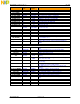
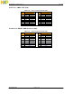
Jumper Default
Posn
PCB
Legend
Description
J51 (CAN
F
)
REMOVED Do not route CAN F to Prototype Area
J52 (CAN D)
REMOVED Do not route CAN D to Prototype Area
J53 (CAN E)
REMOVED Do not route CAN E to Prototype Area
J54 (CAN
C
)
REMOVED Do not route CAN C to Prototype Area
J
55
(INIC
PWR
)
FITTED 2.5v PWR 2.5v is applied to VDDC1 and VDDC2.
J56
(INIC RST)
FITTED RST INIC Reset is connected to PB0
J
57(INIC PS1)
1-2 EVB MLB PS1 is Routed to the EVB INIC
J
58 (INIC /INT)
1-2
EVB /INT is Routed to the EVB INIC
J
59 (INIC SCL)
1-2 EVB SCL is Routed to the EVB INIC
J
60 (INIC BOOT)
1-2 EVB INIC Boot pin is pulled up to 2.5v Rail
J61
(MCU CLK)
1-2 Y2 MCU Clock is Y2
J62
(
PHY PWR
)
FITTED PHY PWR
The DP4348C Ethernet Physical Interface is powered
from the 3.3v SR.
J63
RJ45 No Jumpers
J
64 (
MOST FOT
)
1-2 STATUS MOST FOT is Status is connected to PB1
J
65 (MLBSIG)
1-2 EVB MLBSIG is Routed to the EVB INIC
J66
(MCU CLK)
1-2 Y2 MCU Clock is Y2
J67 (32KHz CLK)
1-2 Y3 32Khz Crystal (Y2) is connected to MCU
J68 (RST-IN)
FITTED
External reset source (LVI, Debug or Target) will be able
to assert MCU reset
J
6
9 (BOOT CFG)
1-2 FLASH MCU boots from internal flash
J70 (TCLK PULL)
1-2
VDDE2
JTAG / NEXUS TCLK signal is pulled to VDDE2 via
10K
Ω
J
71 (32KHz CLK)
1-2 Y3 32Khz Crystal (Y2) is connected to MCU
J72
Not Implemented
J73 (ADC VSUP)
REMOVED Output from variable resistor RV1 is applied to MCU
PA0
J74
REMOVED On board Voltage levels not connected to EVB
J
75 (1
-
2)
FITTED Enables 3.3v board level LVI
J
75 (3
-
4)
FITTED Enables 5v board level LVI
J76 FITTED CLK
PF0 DSPI A CLK is connected to the phantom port
circuitry.
J77
FITTED
SREG
PWR
VDDE2 Domain power is applied to the 4 shift registers
(U15, U16, U21, U22)
J78
FITTED IN
PF1
DSPI_A Serial Data Out
is connected to the phantom
port circuitry.
J79
FITTED CLR
PF11 is connected to the phantom port circuitry. Allows
for software to reset the Shift registers.
J80
FITTED OUT
PF3 DSPI A PCS is connected to the phantom port
circuitry.
J81
(5.0v
-
LINEAR)
FITTED DISABLE 5.0v linear regulator output is Enabled
J82
(
2
.
5v
)
REMOVED DISABLE 2.5v switching regulator output is Enabled
J83
(
3.3v
)
REMOVED DISABLE 3.3v switching regulator output is Enabled
J84
(5.0v)
REMOVED DISABLE 5.0v switching regulator output is Enabled
J
85
(
U20
PWR)
FITTED EVB oscillator module U20 is powered
J86 (RV1)
FITTED
Output from variable resistor RV1 is applied to MCU
PA0
J87
(OSC SEL)
1-2 MOD Daughter card EXT-CLK is routed from U20