
User guide

MPC5668EVB Users Manual Rev 0.1 May 2009
MPC5668EVBUM/D Page 26 of 29
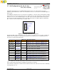
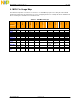
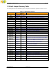
Jumper Default
Posn
PCB
Legend
Description
J
26
(Flex
-
A)
Posn 1-2
FITTED BGE
Flexray-A interface BGE signal is pulled to VIO
J26
(Flex
-
A)
Posn 3-4
FITTED EN
Flexray-A interface EN signal is pulled to VIO
J26
(Flex
-
A)
Posn 5-6
FITTED STBEN
Flexray-A interface STBN signal is pulled to VIO
J26
(Flex
-
A)
Posn 7-8
FITTED WAKE
Flexray-A interface WAKE signal is pulled to GND
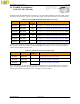
J27 (Flex
-
B
)
Posn 1-2
FITTED TX
MCU PK7 is connected to Flexray B transceiver TX
J27 (Flex
-
B
)
Posn 3-4
FITTED TXEN
MCU PK8 is connected to Flexray B transceiver TXEN
J27(Flex
-
B
)
Posn 5-6
FITTED RX
MCU PK6 is connected to Flexray B transceiver RX
J28
(Flex
-
B)
Posn 1-2
FITTED BGE
Flexray-B interface BGE signal is pulled to VIO
J28
(Flex
-
B)
Posn 3-4
FITTED EN
Flexray-B interface EN signal is pulled to VIO
J28
(Flex
-
B)
Posn 5-6
FITTED STBEN
Flexray-B interface STBN signal is pulled to VIO
J28
(Flex
-
B)
Posn 7-8
FITTED WAKE
Flexray-B interface WAKE signal is pulled to GND
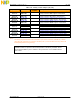
J29 (CAN
-
B
)
Posn 1-2
FITTED TX
MCU CNTX-B is connected to CAN controller C
J
29 (CAN
-
B
)
Posn 3-4
FITTED RX
MCU CNRX-B is connected to CAN controller C
J30 (CAN)
Posn 1-2
FITTED VCC
5v is applied to both CAN transceivers VCC
J30 (CAN)
Posn 3-4
FITTED VIO
Power is applied to both CAN transceivers VIO
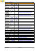
J3
1
(CAN
-
A)
Posn 1-2
FITTED TX
MCU CNTX-A is connected to CAN controller A
J3
1
(CAN
-
A)
Posn 3-4
FITTED RX
MCU CNRX-A is connected to CAN controller A
J32 (JRST)
1-2
BUF
JTAG reset signal is buffered to MCU RESET pin
(connected to the MCU Reset-In circuitry)
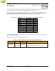
J33
CAN Status – No Jumpers
J34
CAN Status – No Jumpers
J35
FITTED 3.3v PWR 3.3v is applied to VDDP1 and VDDP2 of the INIC
J36
FITTED 2.5v PWR 2.5v is applied to VDDA1 and VDDA2.
J
37
(
MLBCLK
)
1-2 EVB MLBCLK is Routed to the EVB INIC
J38
(
PSO
)
1-2 EVB PSO is Routed to the EVB INIC
J39(MLBDAT)
1-2 EVB MLBDAT is Routed to the EVB INIC
J
40(SDA)
1
-
2
EVB
SDA is Routed to the EVB INIC
J
41
(VDDE
4
)
1-2 5.0v MCU VDDE4 is powered from 5v
J
42
(VDDE
2
)
1-2 5.0v MCU VDDE2 is powered from 5v
J
43
(VDDE
1
)
1-2 5.0v MCU VDDE1 is powered from 5v
J
44
(VDDE
3
)
1-2 5.0v MCU VDDE3 is powered from 5v
J
45 (VDDEMLB)
1-2 2.5V MCU VDD pin is powered from 1.5v switching regulator
J
4
6
(V
RC
)
1
-
2
5V
V
RC
is
supplied from
the
5V switching regulator
J
47
(VRCSEL
)
1-2 INT 3.3 V internal voltage regulator enabled (5 V mode)
J
48
(VDD33)
REMOVED MCU VDD33 pin is powered from switching regulator
J49
(VDDA)
FITTED MCU VDDA is powered from 5V linear regulator
J
50
(VDDSYN)
REMOVED MCU VDDSYN pin is powered from switching regulator