
User guide

MPC5668EVB Users Manual Rev 0.1 May 2009
MPC5668EVBUM/D Page 22 of 29
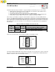
Port J11 is placed on the edge of the EVB to allow the SMSC MOST 150 EVB to be interfaced to the
MPC5668EVB. This allows for evaluation of the MOST150 INIC with the MPC5668. To use this connector the
signals must be routed from the on chip INIC to this connector using the Jumpers detailed in table x below.
Removing these Jumpers also allow the signals between the INIC and the MCU to be isolated.
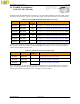
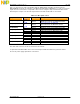
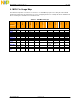
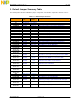
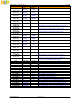
Table 3-23 INIC Signal Control
Jumper
Position
PCB Legend
Description
J37(MLBCLK)
1-2
(D)
EVB MLBCLK is Routed to the EVB INIC
2-3
INIC150 MLBCLK is Routed to the MOST150 header
J38(PSO)
1-2
(D)
EVB
PSO is Routed to the EVB INIC
2-3
INIC150
PSO is Routed to the MOST150 header
J39(MLBDAT)
1-2
(D)
EVB MLBDAT is Routed to the EVB INIC
2-3 INIC150 MLBDAT is Routed to the MOST150 header
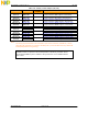
J40(SDA)
1-2
(D)
EVB
SDA
is Routed to the EVB INIC
2-3 INIC150 SDA is Routed to the MOST150 header
J57(PS1)
1-2
(D)
EVB PS1 is Routed to the EVB INIC
2-3 INIC150 PS1 is Routed to the MOST150 header
J58 (/INT)
1-2
(D)
EVB /INT is Routed to the EVB INIC
2-3 INIC150 /INT is Routed to the MOST150 header
J59 (SCL)
1-2
(D)
EVB
SCL is Rout
ed to the EVB INIC
2-3 INIC150 SCL is Routed to the MOST150 header
J65 (MLBSIG)
1-2
(D)
EVB MLBSIG is Routed to the EVB INIC
2-3 INIC150 MLBSIG is Routed to the MOST150 header
The status and reset lines can also be isolated via J56 and J64.
If required the standard fit INIC can be removed and replaced with the ROM memory alternate. Please
observe the power supply requirements of the device.