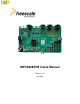
MPC5668EVB Users Manual Revision 0.
MPC5668EVB Users Manual Rev 0.1 May 2009 Revision History: Revision 0.1 Date May 2009 Author D. McMenamin Comment Initial Release, RevA PCB’s only. Information in this document is provided solely to enable system and software implementers to use Freescale Semiconductor products. There are no express or implied copyright licenses granted hereunder to design or fabricate any integrated circuits or integrated circuits based on the information in this document.
MPC5668EVB Users Manual Rev 0.1 May 2009 INDEX 1. INTRODUCTION ...................................................................................................................................................... 1 2. EVB FEATURES ...................................................................................................................................................... 2 3. CONFIGURATION .......................................................................................................
MPC5668EVB Users Manual Rev 0.1 May 2009 Index of Figures and Tables FIGURE 3-1 EVB FUNCTIONAL BLOCKS ............................................................................................................................ 3 FIGURE 3-2 2.1MM POWER CONNECTOR .......................................................................................................................... 4 FIGURE 3-3 2-LEVER POWER CONNECTOR ........................................................................................
MPC5668EVB Users Manual Rev 0.1 May 2009 1. Introduction This user’s manual details the setup and configuration of the Freescale Semiconductor MPC5668 Evaluation Board (hereafter referred to as the EVB). The EVB is intended to provide a mechanism for easy customer evaluation of the MPC5668 family of microprocessors, and to facilitate hardware and software development. At the time of writing this document, the MPC5668 family is offered in a 208MAPBGA package.
MPC5668EVB Users Manual Rev 0.1 May 2009 2. EVB Features The EVB provides the following key features: • • • • • • • • • • • • • • • • • • • • • • MCU Socket supporting the 208BGA production package and the 256BGA development package. Single 12-14V external power supply input with on-board regulators to provide all of the necessary EVB and MCU voltages. Power may be supplied to the EVB via a 2.1mm barrel style power jack or a 2-way level connector. 12V operation allows in-car use if desired.
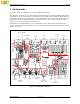
MPC5668EVB Users Manual Rev 0.1 May 2009 3. Configuration This section details the configuration of each of the EVB functional blocks. Throughout this document, all of the default jumper and switch settings are clearly marked with “(D)” and are shown in blue text. This should allow a more rapid return to the default state of the EVB if required. Note that the default configuration for 3-way jumpers is a header fitted between pins 1 and 2.
MPC5668EVB Users Manual Rev 0.1 May 2009 The Power supply section is located in the bottom left area of the EVB 3.1 Power Supply Configuration The EVB requires an external power supply voltage of 12V DC, minimum 1A. This allows the EVB to be easily used in a vehicle if required. The single input voltage is regulated on-board using 3 switching and 1 linear regulators to provide the necessary EVB and MCU operating voltages of 5.0V, 3.3V and 2.5V.
MPC5668EVB Users Manual Rev 0.1 May 2009 3.1.3 Regulator Power Jumpers (J42, J44, J45 and J46) The Power supply control jumpers are located adjacent to the respective regulators. As mentioned above, the EVB has four voltage regulators on board: - 2.5V switching regulator (U17) to supply the MCU MLB Pads voltage and the SMSC INIC (U6). 3.3V switching regulator (U18) for EVB peripherals and MCU regulator, logic and I/O. 5.0V switching regulator (U19) for the MCU regulator and I/O and EVB peripherals. 5.
MPC5668EVB Users Manual Rev 0.1 May 2009 The MCU power supply jumpers are located in the centre of the EVB in a box titled “MCU Supply” 3.1.5 MCU Supply Routing and Jumpers (J41, J42, J43, J44, J45, J46, J47, J48, J49, J50) The MCU can be operated in 5v and 3.3v modes by changing J46. When in 5v mode MCU has internal regulators that can generate the 3.3V supplies for VDDSYN and VDD33.
MPC5668EVB Users Manual Rev 0.1 May 2009 Table 3-2 MCU Power Supply Jumpers Power Domain 5.0V 5.0V / 3.3V Jumper J49 (VDDA) J46 (VRC) J47 (VRCSEL) J43 (VDDE1) J42 (VDDE2) J44 (VDDE3) J41 (VDDE4) 3.3V J48 (VDD33) J50 (VDDSYN) Position PCB Legend FITTED (D) REMOVED MCU VDDA is powered from 5V linear regulator MCU VDDA User powered from J49 Pin 2 1-2 (D) 5V 2-3 1-2 (D) 3.3v INT VRC is supplied from the 3.3V switching regulator 3.
MPC5668EVB Users Manual Rev 0.1 May 2009 3.1.5.1 Changing VDDE[1..4] Voltage Before changing the VDDEx voltage from the default 5.0V setting, you need to ensure that this will not impact any of the EVB peripherals that you are using. The table below details what EVB peripherals are tied to a particular VDDEx grouping and also the MCU pin operating voltage suitable for that peripheral. Table 3-3 VDDE[1..
MPC5668EVB Users Manual Rev 0.1 May 2009 The MCU clock control jumpers are located close to crystal oscillator modules. 3.2 MCU Clock Control 3.2.
MPC5668EVB Users Manual Rev 0.1 May 2009 3.2.2 32Khz External Clock Selection (J67 and J71) The EVB also supports an external 32KHz watch crystal that can be used as a timing source within the MCU. The 32Khz crystal can be optionally connected to PA[14] and PA[15] of the MCU. When using the 32KHz crystal PA[14] and PA[15] will not be visible on P17 Port A header.
MPC5668EVB Users Manual Rev 0.1 May 2009 3.3 Reset Control (Jumper J75) The RESET switch (RED) and LVI circuitry is located to the t left of the MCU in the area titled “RESET “ The EVB incorporates an LVI (Low Voltage Inhibit) device to provide under-voltage protection for the two main switching regulators (5v and 3.3v). When either of these regulator voltages drops below a certain threshold level, the LVI will assert the MCU reset line to prevent incorrect operation of the MCU (or EVB circuitry).
MPC5668EVB Users Manual Rev 0.1 May 2009 3.3.2 Reset Buffering Scheme The MPC5668 family has a single reset pin. This single pin functions as a dual purpose input / output signal, providing Reset-In and Reset-Out functionality. There is a lot of circuitry on the EVB that has access to the reset pin.
MPC5668EVB Users Manual Rev 0.1 May 2009 3.3.3 Reset Boot Configuration (J69) The MPC5668 has a single boot configuration pin (BOOTCFG) which determines the boot location of the MCU based on the state of the pin at POR (Power On Reset). This is shown in the table below: Table 3-10 BOOTCFG Control Jumper Position 1-2 (D) 2-3 J69 (BOOT CFG) PCB Legend FLASH SERIAL Description MCU boots from internal flash MCU boots from external serial source ON 3.
MPC5668EVB Users Manual Rev 0.1 May 2009 3.4.1 Debug Connector Pinouts The EVB is fitted with 14-pin JTAG / ONCE and 38-pin Nexus debug connectors. The following diagram shows the 14-pin JTAG / ONCE connector pinout (0.1” keyed header). TDI 1 TDO3 2 VSS 4 VSS 6 VSS 8 N/C 10 TMS TCLK 5 5v EVTI 7 RESET 9 VDDE2 11 RDY 13 12 VSS 14 JCOMP Figure 3-8.
MPC5668EVB Users Manual Rev 0.1 May 2009 3.5 CAN Configuration (J20, J21, J29, J30, J31) The CAN section is located in the top right corner of the EVB in an area marked “CAN” The EVB has 2x NXP TJA1041T high speed CAN transceiver on the MCU CAN-A and CAN-B channels. These can operate with 5v or 3.3v I/O from the MCU. This is determined by VDDE2 domain. For flexibility, the CAN transceiver I/O is connected to a standard 0.1” connector and DB9 connector at the top edge of the PCB.
MPC5668EVB Users Manual Rev 0.1 May 2009 3.6 RS232 Configuration (J6, J17, J18, J23, J24) The RS232 circuitry is located at the top edge of the EVB in an area titled “SCI” The EVB has a single MAX3223 RS232 transceiver device, providing RS232 signal translation for the MCU SCI channels A and B. Each of the two RS232 outputs from the MAX232 device is connected to a DB9 connector, allowing a direct RS232 connection to a PC or terminal.
MPC5668EVB Users Manual Rev 0.1 May 2009 3.7 LIN Configuration (J3, J4, J5, J12, J13, J14, J15,J16) The LIN circuitry is located in the top edge of the EVB in an area titled “LIN” The EVB is fitted with two Freescale MCZ33661EF LIN transceivers. The eSCI module incorporates a hardware controlled LIN master, and as such, the LIN transceivers are connected to the TX and RX signals of SCI C and D. For flexibility, the LIN transceivers are connected to a standard 0.
MPC5668EVB Users Manual Rev 0.1 May 2009 The Flexray circuitry is located in the top edge of the EVB in an area titled “Flexray” 3.8 FlexRAY Configuration (J19, J27, J25, J26, J28) The EVB is fitted with 2 FlexRAY physical interfaces connected to MCU FlexRAY channels A and B. Jumpers J19 and J27 are provided to route the respective MCU signals to the physical interfaces as described below.
MPC5668EVB Users Manual Rev 0.
MPC5668EVB Users Manual Rev 0.1 May 2009 The Ethernet circuitry is located in the right edge of the EVB in an area titled “Ethernet” 3.9 Ethernet The EVB is fitted with a National Semiconductor DP8348C Ethernet physical interface (U9) and a Pulse Jack J1011F21PNL RJ45 connector with integrated activity LED’s and magnetics (J63). The National Semiconductor DP8348C physical interface is connected to the MII on the MPC5668. This is a fixed connection with no means of isolation.
MPC5668EVB Users Manual Rev 0.1 May 2009 The MLB and MOST circuitry is located on the left edge of the EVB . 3.10 MLB and Most The EVB is fitted with a range of hardware to support the MOST communication protocol. These include: SMSC OS81050 (U6) INIC interfaced to the MPC5668 via 3 pin Media Local Bus (MLB) interface.
MPC5668EVB Users Manual Rev 0.1 May 2009 Port J11 is placed on the edge of the EVB to allow the SMSC MOST 150 EVB to be interfaced to the MPC5668EVB. This allows for evaluation of the MOST150 INIC with the MPC5668. To use this connector the signals must be routed from the on chip INIC to this connector using the Jumpers detailed in table x below. Removing these Jumpers also allow the signals between the INIC and the MCU to be isolated.
MPC5668EVB Users Manual Rev 0.1 May 2009 3.11 Phantom Ports (J76, J77, J78, J79, J80) The Phantom port circuitry is located on the bottom edge of the EVB To support the de-serialisation feature of the MPC5668 DSPI module, the EVB features 4 chained SIPO shift registers interfaced to DSPI A. This allows a 32-bit phantom port to be created. The port can operate at either 5V or 3.3V depending on the VDDE2 supply voltage (J42). This is outputted on P24 and P25.
MPC5668EVB Users Manual Rev 0.1 May 2009 4. MCU Pin Usage Map The table below provides a useful cross reference to see what MCU port pins are used by the various EVB peripherals and functions. Note that there are some overlapping functions for example the Nexus and External bus as shown by the shaded boxes in the table below. Table 4-1. EVB MCU Pin Usage Port k Port J Port H PD[0..1] PD[2..3] PD[12,13] PD[14,15] PE[0,1] PE[2,3] PK[3..5] PK[6..8] PK[9] PG[6..9] PG[12..15] PG[0] PG[2..
MPC5668EVB Users Manual Rev 0.1 May 2009 5. Default Jumper Summary Table The following table details the DEFAULT jumper configuration of the EVB as explained in detail in section 3.
MPC5668EVB Users Manual Rev 0.
MPC5668EVB Users Manual Rev 0.1 Jumper Default Posn May 2009 PCB Legend J51 (CAN F) J52 (CAN D) J53 (CAN E) J54 (CAN C) J55 (INIC PWR) J56 (INIC RST) J57(INIC PS1) J58 (INIC /INT) J59 (INIC SCL) J60 (INIC BOOT) J61 (MCU CLK) J62 (PHY PWR) REMOVED REMOVED REMOVED REMOVED FITTED FITTED 1-2 1-2 1-2 1-2 1-2 2.
MPC5668EVB Users Manual Rev 0.1 May 2009 The user connectors are located on the right hand side of the PCB 6. User Connector Descriptions This section details the pinout of the EVB user connectors. The connectors are 0.1 inch pitch turned pin headers and are located to the right hand side of the EVB. Pins are grouped by port functionality and the PCB legend shows the respective port number adjacent to each pin. 6.1.1 Port A / ADC (Connector J86, RV1, J73 and J74) Table 6-1.
MPC5668EVB Users Manual Rev 0.1 May 2009 6.1.2 Port B / ADC / SPI (P18) Table 6-3. Port B Connector Pinout (P18) Pin Function st GPIO 1 Alt Pin Function st GPIO 1 Alt 1 3 5 7 9 11 13 15 17 PB0 AN16 PB2 AN18 PB4 AN20 PB6 AN22 PB8 AN24 PB10 AN26 PB12 AN28 PB14 AN30 GND 2 4 6 8 10 12 14 16 18 PB1 AN17 PB3 AN19 PB5 AN21 PB7 AN23 PB9 AN25 PB11 AN27 PB13 AN29 PB15 AN31 GND 6.1.3 Port C / ADC / FLEXRAY / I2C (P19) Table 6-4.
MPC5668EVB Users Manual Rev 0.1 May 2009 6.1.5 Port E / SCI / eMIOS / I2C (P21) Table 6-6. Port E Connector Pinout (P21) Pin 1 3 5 7 9 11 13 15 17 Function st GPIO 1 Alt PE0 PE2 PE4 PE6 PE8 PE10 PE12 PE14 TXD_C TXD_D TXD_E TXD_F TXD_G TXD_H TXD_J SCL_A GND Pin 2 4 6 8 10 12 14 16 18 Function st GPIO 1 Alt PE1 PE3 PE5 PE7 PE9 PE11 PE13 PE15 RXD_C RXD_D RXD_E RXD_F RXD_G RXD_H RXD_J SDA_A GND 6.1.6 Port F / DSPI (P26) Table 6-7.
MPC5668EVB Users Manual Rev 0.1 May 2009 6.1.9 Port J / eMIOS / FEC (P29) Table 6-10. Pin 1 3 5 7 9 11 13 15 17 Port J Connector Pinout (P29) Function GPIO 1st Alt PJ0 PJ2 PJ4 PJ6 PJ8 PJ10 PJ12 PJ14 Pin 2 4 6 8 10 12 14 16 18 eMIOS[15] eMIOS[13] eMIOS[11] eMIOS[9] eMIOS[7] eMIOS[5] eMIOS[3] eMIOS[1] GND Function GPIO 1st Alt PJ1 PJ3 PJ5 PJ7 PJ9 PJ11 PJ13 PJ15 eMIOS[14] eMIOS[12] eMIOS[10] eMIOS[8] eMIOS[6] eMIOS[4] eMIOS[2] eMIOS[0] GND 6.1.10 Port K / RESET / MLB (Connector P30) Table 6-11.
MPC5668EVB Users Manual Rev 0.1 May 2009 The prototyping area is located on the right hand side of the EVB, above the user connectors. 6.2 Prototyping Area and User LED’s / Switches There is a rectangular prototype area on the EVB, consisting of a 0.1inch pitch array of through-hole plated pads. Power from all three voltage regulators is readily accessible along with GND. This area is ideal for the addition of any custom circuitry. Adapters are available to convert SMD devices to 0.
MPC5668EVB Users Manual Rev 0.
MPC5668EVB Users Manual Rev 0.
MPC5668EVB Users Manual Rev 0.
MPC5668EVB Users Manual Rev 0.
MPC5668EVB Users Manual Rev 0.
MPC5668EVB Users Manual Rev 0.
MPC5668EVB Users Manual Rev 0.
MPC5668EVB Users Manual Rev 0.
MPC5668EVB Users Manual Rev 0.
MPC5668EVB Users Manual Rev 0.
MPC5668EVB Users Manual Rev 0.
MPC5668EVB Users Manual Rev 0.
MPC5668EVB Users Manual Rev 0.
MPC5668EVB Users Manual Rev 0.
MPC5668EVB Users Manual Rev 0.
MPC5668EVB Users Manual Rev 0.
MPC5668EVB Users Manual Rev 0.
MPC5668EVB Users Manual Rev 0.