
Datasheet


Electrical characteristics
i.MX 8QuadXPlus and 8DualXPlus Automotive and Infotainment Applications Processors, Rev. 0, 11/2018
PRELIMINARYNXP Semiconductors 93
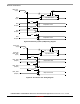
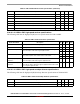
Figure 50. JTAG_TRST_B Timing Diagram
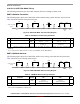
4.10.14 SPDIF Timing Parameters
The Sony/Philips Digital Interconnect Format (SPDIF) data is sent using the bi-phase marking code. When
encoding, the SPDIF data signal is modulated by a clock that is twice the bit rate of the data signal.
Table 90, Figure 51, and Figure 52 show SPDIF timing parameters for the Sony/Philips Digital
Interconnect Format (SPDIF), including the timing of the modulating Rx clock (SPDIF_SR_CLK) for
SPDIF in Rx mode and the timing of the modulating Tx clock (SPDIF_ST_CLK) for SPDIF in Tx mode.
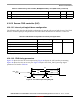
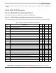
Table 89. JTAG Timing
ID Parameter
1,2
All Frequencies
Unit
Min Max
SJ0 JTAG_TCK frequency of operation 1/(3xT
DC
)
1
1
T
DC
= target frequency of SJC
0.001 22 MHz
SJ1 JTAG_TCK cycle time in crystal mode 45 — ns
SJ2 JTAG_TCK clock pulse width measured at
V
M
2
2
V
M
= mid-point voltage
22.5 — ns
SJ3 JTAG_TCK rise and fall times — 3 ns
SJ4 Boundary scan input data set-up time 5 — ns
SJ5 Boundary scan input data hold time 24 — ns
SJ6 JTAG_TCK low to output data valid — 40 ns
SJ7 JTAG_TCK low to output high impedance — 40 ns
SJ8 JTAG_TMS, JTAG_TDI data set-up time 5 — ns
SJ9 JTAG_TMS, JTAG_TDI data hold time 25 — ns
SJ10 JTAG_TCK low to JTAG_TDO data valid — 44 ns
SJ11 JTAG_TCK low to JTAG_TDO high impedance — 44 ns
SJ12 JTAG_TRST_B assert time 100 — ns
SJ13 JTAG_TRST_B set-up time to JTAG_TCK low 40 — ns
JTAG_TCK
(Input)
(Input)
SJ13
SJ12
JTAG_TRST_B