
Datasheet


Electrical characteristics
i.MX 8QuadXPlus and 8DualXPlus Automotive and Infotainment Applications Processors, Rev. 0, 11/2018
PRELIMINARYNXP Semiconductors 91
4.10.13 Secure JTAG controller (SJC)
4.10.13.1 Internal pull-up/pull-down configuration
The following table describes the default configuration of internal pull-ups and pull-downs of the JTAG
interface. External pull-ups and pull-downs are needed when this interface is routed to a connector.
4.10.13.2 JTAG timing parameters
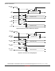
Figure 47 depicts the SJC test clock input timing. Figure 48 depicts the SJC boundary scan timing.
Figure 49 depicts the SJC test access port. Figure 50 depicts the JTAG_TRST_B timing. Signal
parameters are listed in Table 89.
Figure 47. Test Clock Input Timing Diagram
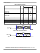
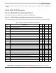
t9 QSPI
x
[A/B]_DATA
y
Setup Time 0.65 — ns
t10 QSPI
x
[A/B]_DATA
y
Hold Time 0.65 — ns
1
Timing is controlled from FLSH
x
CR1 register (
x
=A1, A2, B1, or B2).
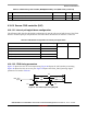
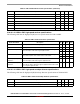
Table 88. JTAG default configuration for internal pull-up/pull-down
Ball name Internal pull setting
1
1
PU = pull-up; PD = pull-down
Typical pull value Unit
JTAG_TMS PU 50 KΩ
JTAG_TCK PD
JTAG_TDI PU
JTAG_TRST_B PU
TEST_MODE_SELECT PD
Table 87. FlexSPI timings with FlexSPI
n
_MCR0[RXCLKSRC] = 0x3 (DDR mode)
(continued)
ID Parameter Min Max Unit
JTAG_TCK
(Input)
VM
VM
VIH
VIL
SJ1
SJ2
SJ2
SJ3
SJ3