
Datasheet


Electrical characteristics
i.MX 8QuadXPlus and 8DualXPlus Automotive and Infotainment Applications Processors, Rev. 0, 11/2018
PRELIMINARYNXP Semiconductors 89
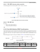
4.10.12.2 DDR mode
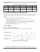
4.10.12.2.1 DDR mode timing diagrams
Figure 44. FlexSPI write timing diagram (DDR mode)
Figure 45. FlexSPI read timing diagram (DDR mode)
Figure 46. FlexSPI read with DQS timing diagram (DDR mode)
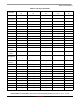
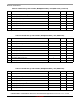
Table 85. FlexSPI timings with FlexSPI
n
_MCR0[RXCLKSRC] = 0x0 (DDR mode)
ID Parameter Min Max Unit
— QSPI
x
[A/B]_SCLK Cycle frequency — 30 MHz
t1 QSPI
x
[A/B]_SCLK High or Low Time 15 — ns