
Datasheet


Electrical characteristics
i.MX 8QuadXPlus and 8DualXPlus Automotive and Infotainment Applications Processors, Rev. 0, 11/2018
PRELIMINARYNXP Semiconductors 87
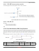
The following read timing diagram is valid for FlexSPIn_MCR0[RXCLKSRC] = 0x0 or 0x1.
Figure 42. FlexSPI read timing diagram (SDR mode)
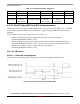
The following read timing diagram is valid for FlexSPIn_MCR0[RXCLKSRC] = 0x3.
Figure 43. FlexSPI read with DQS timing diagram (SDR mode)
4.10.12.1.2 SDR mode timing parameter tables
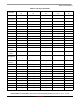
Table 82. FlexSPI timings with FlexSPI
n
_MCR0[RXCLKSRC] = 0x0 (SDR mode)
ID Parameter Min Max Unit
— QSPI
x
[A/B]_SCLK Cycle frequency — 60 MHz
t1 QSPI
x
[A/B]_SCLK High or Low Time 7.5 — ns
t2 QSPI
x
[A/B]_SS
y
_B pulse width 1 — SCLK
t3 QSPI
x
[A/B]_SS
y
_B Lead Time
1
1
Timing is controlled from FLSH
x
CR1 register (
x
=A1, A2, B1, or B2).
TCSS+0.5 — SCLK
t4 QSPI
x
[A/B]_SS
y
_B Lag Time
1
TCSH — SCLK
t5 QSPI
x
[A/B]_DATA
y
output Delay — 1 ns
t6 QSPI
x
[A/B]_DATA
y
Setup Time 6 — ns
t7 QSPI
x
[A/B]_DATA
y
Hold Time 0 — ns