
Datasheet


Electrical characteristics
i.MX 8QuadXPlus and 8DualXPlus Automotive and Infotainment Applications Processors, Rev. 0, 11/2018
PRELIMINARY NXP Semiconductors86
4.10.12 FlexSPI (Quad SPI/Octal SPI) timing parameters
The FlexSPI interface can work in SDR or DDR modes. It can operate up to 60 MHz at 3.3 V, 166 MHz
at 1.8 V SDR mode or 200 MHz at 1.8 V DDR mode. It supports single-ended and differential DQS
signaling.
FlexSPI supports the following clocking scheme for a read data path:
• Dummy read strobe generated by FlexSPI controller and looped back internally
(FlexSPIn_MCR0[RXCLKSRC] = 0x0)
• Dummy read strobe generated by FlexSPI controller and looped back through the DQS pad
(FlexSPIn_MCR0[RXCLKSRC] = 0x1). It means the I/O cannot be used for another feature.
• Read strobe provided by memory device and input from DQS pad
(FlexSPIn_MCR0[RXCLKSRC] = 0x3)
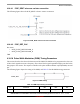
4.10.12.1 SDR mode
4.10.12.1.1 SDR mode timing diagrams
The following write timing diagram is valid for any FlexSPIn_MCR0[RXCLKSRC] value.
Figure 41. FlexSPI write timing diagram (SDR mode)
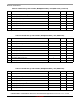
LCD_D1 B[1] B[1] B[1] B[1] Y/C[1]
LCD_D0 B[0] B[0] B[0] B[0] Y/C[0]
LCD_RESET LCD_RESET LCD_RESET LCD_RESET LCD_RESET —
LCD_BUSY /
LCD_VSYNC
LCD_BUSY (or
optional
LCD_VSYNC)
LCD_BUSY (or
optional LCD_VSYNC)
LCD_BUSY (or
optional
LCD_VSYNC)
LCD_BUSY (or
optional
LCD_VSYNC)
—
Table 81. LCD Signal Parameters (continued)