
Datasheet


Electrical characteristics
i.MX 8QuadXPlus and 8DualXPlus Automotive and Infotainment Applications Processors, Rev. 0, 11/2018
PRELIMINARY NXP Semiconductors84
4.10.11 LCD controller (LCDIF) parameters
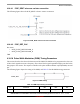
Figure 40 shows the LCDIF timing, and Table 80 lists the timing parameters.
Figure 40. LCD Timing
4.10.11.1 LCDIF signal mapping
Table 81 lists the details about the mapping signals.
P1 PWM output pulse width high 15 — ns
P2 PWM output pulse width low 15 — ns
Table 80. LCD Timing Parameters
ID Parameter Symbol Min Max Unit
L1 LCD pixel clock frequency tCLK(LCD) — 80 MHz
L2 LCD pixel clock high (falling edge capture) tCLKH(LCD) 6 — ns
L3 LCD pixel clock low (rising edge capture) tCLKL(LCD) 6 — ns
L4 LCD pixel clock high to data valid (falling edge capture) td(CLKH-DV) -1 1 ns
L5 LCD pixel clock low to data valid (rising edge capture) td(CLKL-DV) -1 1 ns
L6 LCD pixel clock high to control signal valid (falling edge capture) td(CLKH-CTRLV) -1 1 ns
L7 LCD pixel clock low to control signal valid (rising edge capture) td(CLKL-CTRLV) -1 1 ns
Table 79. PWM Output Timing Parameters (continued)
/ / /
/
/&'QB&/.
IDOOLQJHGJHFDSWXUH
/&'QB&/.
ULVLQJHGJHFDSWXUH
/&'QB'$7$>@
/&'Q&RQWURO6LJQDOV
/
/
/