
Datasheet


Electrical characteristics
i.MX 8QuadXPlus and 8DualXPlus Automotive and Infotainment Applications Processors, Rev. 0, 11/2018
PRELIMINARYNXP Semiconductors 83
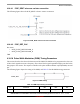
4.10.9.1 PCIE_REXT reference resistor connection
The following figure shows the PCIE_REXT reference resistor connection.
Figure 38. PCIE_REXT reference resistor connection
4.10.9.2 PCIE_REF_CLK
Pin names:
• PCIE_[SATA]_REFCLK100M_P
• PCIE_[SATA]_REFCLK100M_N
TBD
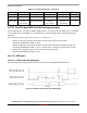
4.10.10 Pulse Width Modulator (PWM) Timing Parameters
This section describes the electrical information of the PWM. The PWM can be programmed to select one
of three clock signals as its source frequency. The selected clock signal is passed through a prescaler before
being input to the counter. The output is available at the pulse-width modulator output (PWMO) external
pin.
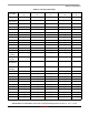
The following figure depicts the timing of the PWM, and Table 79 lists the PWM timing parameters.
Figure 39. PWM Timing
Table 79. PWM Output Timing Parameters
ID Parameter Min Max Unit
— PWM Module Clock Frequency 0 ipg_clk MHz
PWMn_OUT