
Datasheet


Electrical characteristics
i.MX 8QuadXPlus and 8DualXPlus Automotive and Infotainment Applications Processors, Rev. 0, 11/2018
PRELIMINARY NXP Semiconductors82
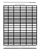
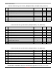
Table 78. PCIe differential output driver characteristics (including board and load)
Parameter Min Typ Max Units Notes
Output Rise and fall time T
R
, T
F
175 — 350 ps
1
1
When the output is transitioning between logic 0 and logic 1, or logic 1 and logic 0, and driving a terminated
transmission line, the outputs monotonically transition between VOL and VOH, VOH, and VOL respectively. Target rise and
fall times observed at the receiver and are primarily set by board trace impedance and Load capacitance. Rise and fall
times are defined by 25% and 75% crossing points.
Output Rise/Fall matching — — 20 %
1,
2
2
Calculated as: 2 × (TR–TF) / (TR+ TF)
Output skewT
OSKEW
— — 50 ps —
Initialization time from assertion of TXOE 100 — — ns —
Initialization time from assertion of TXENA — 10 — μs—
Transmission line characteristic impedance (Z
O
)—50—Ω —
Driver output impedance, single ended (small signal @
Vout=Vcm)
— 1000 — Ω —
Output single ended voltage (RS= 33, RT= 50 Ω)
V
OH
I
OH
@ 6 * I
R
V
OL
0.65
-13
-0.20
0.71
-14.2
0.00
0.85
-17
0.05
V
mA
V
3, 4
3
3
I
R
is proportional to the reference current. Measured across RT. The primary contributor to output voltage spread is
VDD spread, and so a VDD tighter than ±10% may be required to achieve this spread.
4
Higher output voltages may occur depending on load, power supply, and selected output drive. Higher output voltages may
transiently occur during initialization period following TXENA assertion.
Output common mode voltage (RS = 33, RT= 50 Ω)
|V
OCM
|
ΔV
OCM (DC)
ΔV
OCM (AC)
0.25
-0.015
-0.050
0.375 0.55
0.015
0.050
V
5
6
5
Peak change in output differential voltage when driving a logic 0 and when driving a logic 1 under DC conditions.
6
Peak change in output differential voltage when driving a logic 0 and when driving a logic 1 under AC conditions.
Buffer induced deterministic jitter (absolute, pk-pk) — — 4 ps
7,8
7
Measured under “clean power supply and ground” conditions, and after de-embedding the jitter of the input, measured over a
time span of 1000 cycles
8
Power supply induced jitter is included under this category, and the power supply variation is to be less than 8mVpp.
Note that customer has to be uncommonly careful with power supply fidelity due to the small jitter numbers.
Reference Buffer Dynamic Power (Digital) — 0.015 0.66 μA
9
9
Power consumption is simulated under the following conditions:
Typ: TT, VDD=1.0 V, VD18=1.8 V, 25 °C
Max: FF, VDD=1.1 V, VD18=1.98 V, 125 °C
Dynamic: TXENA=1, TXOE=1
Static: TXENA=0, TXOE=1
Reference Buffer Dynamic Power (Analog) — 2.8 3.14 mA
9
Output Buffer Dynamic Power (Digital) — 0.035 1.8 μA
9
Output Buffer Dynamic Power (Analog) — 18.9 22.11 mA
9